Xenon Difluoride XeF₂ Selectivity: How Xenon Difluoride Achieves Precision Etching Without Damaging Microstructures
BY Tao, Published Jan 3, 2026
In the intricate, nanometer-scale world of semiconductor manufacturing and Micro-Electro-Mechanical Systems (MEMS), the ability to remove material is commonplace. We have dozens of ways to blast, dissolve, or erode silicon. However, the true art of microfabrication lies not in what you remove, but in what you preserve.
This is the domain of selectivity.
Over the past 3 years, China Isotope Development Co Ltd was starting to supply Xenon Difluoride (XeF₂) to China domestic clients, I have witnessed the evolution of etching technologies from wet chemical baths to high-density plasma systems. Yet, among all these methods, Xenon Difluoride (XeF₂) stands apart as a unique chemical anomaly. It offers a capability that seems almost counter-intuitive: the ability to devour silicon with aggressive speed while leaving materials like silicon dioxide, silicon nitride, aluminum, and even delicate photoresists virtually untouched.
Hopefully, this article can be a deep dive into the science of selectivity. We will explore the chemical and physical mechanisms that allow XeF₂ to achieve “surgical” precision, ensuring the integrity of complex microstructures. We will move beyond the basic datasheet numbers to understand why this molecule behaves the way it does, and how engineers harness this behavior to build the impossible.
1. The Definition of Selectivity in Microfabrication
Before analyzing the chemistry, we must rigorously define our terms. In semiconductor processing, selectivity (𝑆) is a dimensionless ratio comparing the etch rate of the target material (Silicon) to the etch rate of the masking or structural material (M).
𝑆=𝑅𝑆𝑖𝑅𝑀
- 𝑅𝑆𝑖: Etch rate of Silicon (e.g., 𝜇𝑚/𝑚𝑖𝑛).
- 𝑅𝑀: Etch rate of the mask/stop layer (e.g., 𝐴˚/𝑚𝑖𝑛).
In conventional Plasma Enhanced Reactive Ion Etching (RIE), achieving a selectivity of 50:1 or 100:1 is considered excellent. This means for every 100 microns of silicon removed, you lose 1 micron of your mask.
With Xenon Difluoride, we routinely observe selectivity ratios exceeding 1,000:1, and in optimized conditions, 5,000:1 or even higher.
This is not merely an incremental improvement; it is a fundamental shift in processing capability. It means you can etch through an entire silicon wafer and stop on a layer of oxide less than 100 nanometers thick without puncturing it. It means you can release a MEMS gyroscope suspended by springs thinner than a human hair, without degrading the mechanical properties of those springs.
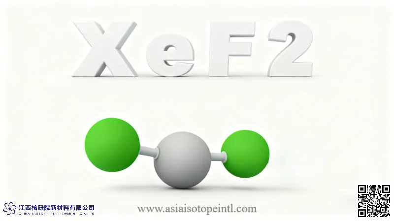
But how does a simple triatomic molecule (𝐹−𝑋𝑒−𝐹) make such intelligent decisions?
2. The Chemical Engine: The Spontaneous Reaction
The secret to XeF₂’s selectivity lies in its reaction mechanism. Unlike plasma etching, which relies on “brute force” ion bombardment to break bonds, XeF₂ etching is a purely chemical, thermodynamically driven process.
The Reactant: A Noble Gas with a Grudge
Xenon is a noble gas, generally inert. However, fluorine is the most electronegative element in the universe. When forced together to form XeF₂, the molecule is stable but reactive. The bond between Xenon and Fluorine is relatively weak compared to the bond Fluorine can form with Silicon.
The Mechanism: Adsorption and Disproportionation
The reaction proceeds in a specific sequence at the silicon surface:
- Physisorption: The XeF₂ molecule lands on the silicon surface. It doesn’t need high energy to get there; it simply diffuses.
- Dissociation: The molecule breaks apart. The fluorine atoms dissociate from the xenon.
- Fluorination: The fluorine atoms form bonds with the surface silicon atoms.
- Product Formation: Once a silicon atom is surrounded by four fluorine atoms, it forms Silicon Tetrafluoride (SiF₄).
- Desorption: SiF₄ is a gas with a high vapor pressure. It immediately detaches from the surface and floats away. The Xenon atom (𝑋𝑒) also returns to the gas phase.
The chemical equation is clean and residue-free: 2𝑋𝑒𝐹2(𝑔𝑎𝑠)+𝑆𝑖(𝑠𝑜𝑙𝑖𝑑)→𝑆𝑖𝐹4(𝑔𝑎𝑠)+2𝑋𝑒(𝑔𝑎𝑠)
The critical takeaway here is spontaneity. This reaction is exothermic (it releases heat) and has a very low activation energy barrier on silicon. It happens automatically at room temperature.
3. The Thermodynamics of “No”: Why It Ignores Other Materials
Selectivity is not just about what reacts; it is about what doesn’t react. Why does XeF₂ destroy silicon but bounce harmlessly off Silicon Dioxide (SiO₂) or Silicon Nitride (Si₃N₄)?
The answer lies in Bond Dissociation Energy (BDE).
The Fortress of Oxygen
To etch Silicon Dioxide (𝑆𝑖𝑂2), the etchant must break the Silicon-Oxygen bond to replace it with a Silicon-Fluorine bond.
- Si-F Bond Energy: ~553 kJ/mol (This is the driving force).
- Si-O Bond Energy: ~799 kJ/mol (This is the barrier).
Thermodynamically, the Si-O bond is stronger than the Si-F bond. The XeF₂ molecule simply does not carry enough internal chemical energy to break the existing Si-O bond. In a plasma system, we supply external energy (via accelerated ions) to smash that bond physically. But in a simplified XeF₂ vapor system, there are no ions. There is no external kinetic energy.
Therefore, the reaction with SiO₂ is thermodynamically unfavorable. The XeF₂ molecule adsorbs onto the oxide surface, “realizes” it cannot break the bond, and eventually desorbs unchanged.
The Implications for Process Integration
This thermodynamic reality is why XeF₂ is the gold standard for CMOS-MEMS integration.
- Gate Oxides: Even ultra-thin gate oxides are safe.
- Passivation Layers: Standard Nitride passivation layers are impenetrable barriers.
- Photoresist: Most organic photoresists do not have the specific binding sites to trigger the fluorine transfer efficiently, allowing standard lithography resists (like SU-8 or positive resists) to act as perfect masks without the need for complex “hard masks” like Chromium or Gold.

4. The Absence of Ion Bombardment: The “Soft Touch”
To truly understand selectivity, we must contrast XeF₂ with its rival: Deep Reactive Ion Etching (DRIE).
In DRIE (the Bosch process), the system alternates between etching and polymer deposition. High-energy ions are accelerated toward the wafer to punch through the polymer at the bottom of the trench.
- The Problem: These ions are like microscopic bullets. When they hit the mask material (oxide or resist), they physically sputter it away. Even if the chemistry doesn’t attack the mask, the physics does.
- The Damage: This ion bombardment causes lattice damage, charge accumulation (which can destroy sensitive transistors), and mask erosion.
XeF₂ is an Ion-Free Zone. Because XeF₂ etching is purely chemical (isotropic), there is no physical sputtering.
- Zero Sputtering: The mask is not physically worn down. This allows for extremely long etch times (hours) without mask failure.
- Zero Charging: Since there is no plasma, there are no charged particles bombarding the device. This is critical for Failure Analysis (FA) of active integrated circuits, where introducing a charge could alter the electrical properties of the transistors being studied.
5. Selectivity with Metals: The Passivation Phenomenon
The interaction between XeF₂ and metals is nuanced and fascinating. While XeF₂ is an oxidizer, it exhibits remarkable selectivity to common semiconductor metals like Aluminum (Al), Copper (Cu), and Gold (Au).
Why doesn’t the Fluorine attack the Aluminum? Technically, it starts to.
When XeF₂ meets Aluminum, it forms Aluminum Fluoride (AlF₃). Unlike SiF₄ (which is a gas and flies away), AlF₃ is a solid, non-volatile salt. 2𝐴𝑙+3𝑋𝑒𝐹2→2𝐴𝑙𝐹3(𝑠𝑜𝑙𝑖𝑑)+3𝑋𝑒
This thin layer of AlF₃ forms on the surface of the aluminum. Once it is a few angstroms thick, it acts as a passivation layer—a shield. It prevents further XeF₂ molecules from reaching the fresh aluminum underneath. The reaction chokes itself off.
The “Dirty” Metals: It is important to note, as a scientist, that selectivity is not infinite for all metals.
- Titanium (Ti) and Tungsten (W): These metals form fluorides that are somewhat volatile or do not passivate well. They will etch in XeF₂, albeit slower than silicon.
- Molybdenum (Mo) and Germanium (Ge): These etch very rapidly in XeF₂. If your device uses Mo or Ge, XeF₂ is likely not the right tool (or requires very specific sacrificial layer strategies).
Understanding this “Metallurgical Selectivity” is vital for packaging and interconnect preservation.
6. Factors Influencing Selectivity in the Fab
While the intrinsic chemistry offers high selectivity, the actual selectivity achieved in the fabrication plant depends on process parameters.
Temperature Effects
XeF₂ etching is exothermic. The reaction generates heat.
- Runaway Effect: If the silicon wafer gets too hot (>100°C) due to the reaction heat, the chemical resistance of the mask materials (like photoresist) can degrade. The resist might soften or burn, failing mechanically rather than chemically.
- Solution: This is why modern XeF₂ systems use Pulsed Etching. By introducing the gas in short pulses and evacuating, we allow the heat to dissipate, keeping the substrate near room temperature and maintaining maximum selectivity.
The “Loading Effect”
The etch rate of silicon depends on the exposed surface area. A wafer with 90% exposed silicon acts as a massive “sink” for fluorine atoms, lowering the effective pressure. While this slows down the silicon etch rate, it paradoxically can help selectivity. Because the fluorine is so eager to react with the abundant silicon, it has even less statistical probability of attacking the mask material.
However, towards the end of a release etch, when the sacrificial silicon is almost gone, the concentration of XeF₂ rises. This is the “over-etch” period. It is during this phase that the high selectivity of XeF₂ is most critical, as the full chemical potential is now interacting with the structural layers.
7. Real-World Applications of High Selectivity
The theoretical advantages of XeF₂ selectivity translate into specific engineering capabilities that enable modern technology.
1. The “Release” of MEMS Micro-Mirrors
Consider the Digital Micromirror Device (DMD) used in cinema projectors. Millions of aluminum mirrors sit on tiny torsion hinges.
- The Challenge: Remove the sacrificial layer under the mirror without pitting the mirror surface (smoothness affects optical quality) or weakening the hinge (durability).
- The XeF₂ Solution: The >1000:1 selectivity to Aluminum allows the silicon underneath to be completely evacuated, leaving the optical finish of the mirror pristine.
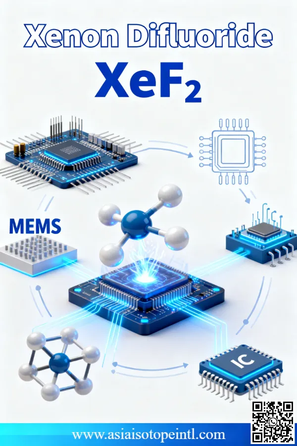
2. CMOS-MEMS Monolithic Integration
Engineers often want to build sensors directly on top of the computer chip that processes the signal.
- The Challenge: You cannot expose the underlying CMOS transistors to plasma (charging damage) or high heat (dopant diffusion).
- The XeF₂ Solution: Using the high selectivity to SiO₂ and Si₃N₄ (the passivation layers of the chip), XeF₂ removes the MEMS sacrificial layer without ever touching the sensitive electronics millimeters below.
3. Delayering for Failure Analysis
When an Intel or Samsung chip fails, analysts need to strip it layer by layer to find the fault.
- The Challenge: Remove the polysilicon gate material without damaging the ultra-thin Gate Oxide underneath.
- The XeF₂ Solution: The immense selectivity allows analysts to stop the etch exactly on the oxide interface, preserving the physical evidence of the failure mechanism (e.g., a pinhole in the oxide).
8. Conclusion: The Power of Chemical Intelligence
In the toolset of the semiconductor engineer, Xenon Difluoride is not a hammer; it is a scalpel. Its power comes not from physical force, but from chemical intelligence.
By exploiting the fundamental thermodynamic differences between Silicon-Fluorine bonds and Silicon-Oxygen/Nitrogen bonds, XeF₂ achieves a level of material discrimination that plasma processes cannot match. It allows us to reach into the microscopic world and subtract material with atomic precision, respecting the boundaries of the structures we wish to preserve.
For the fabrication of next-generation sensors, the integration of 3D stacked chips, and the forensic analysis of nanometer-scale logic, understanding and utilizing the selectivity of XeF₂ is not just an option—it is a necessity. It is the invisible chemical key that unlocks the release of the complex mechanical world from the static solid block.
Would you like a deeper dive into any specific technical parameters or applications?
As an industry leader focused in Specialty Gases products, our goal is to support our customers by keeping them at the forefront of their industries. We’re here to help with any questions you might have so you can transform your ideas into reality, and tackle those big science challenges.
Get free consultant, our experts are ready to serve.
(Follow up our update articles on www.asiaisotopeintl.com or send your comments to tao.hu@asiaisotope.com for further communications)