Xenon Difluoride in Semiconductor Chip Repair: A Precision Tool for Nanoscale Circuit Modification
BY Tao, Published Jan 3, 2026
Introduction: The High-Stakes World of Nanoscale Surgery
In the semiconductor industry, the margin for error is measured in atoms. As we push logic nodes toward 5nm, 3nm, and the Angstrom era, the complexity of Integrated Circuits (ICs) has exploded. A single modern GPU or AI processor can contain over 100 billion transistors. But what happens when a design flaw is discovered after the first batch of prototypes—the “first silicon”—arrives from the foundry?
You cannot simply use a soldering iron to fix a chip where the wires are a thousand times thinner than a human hair. The cost of generating a new set of photomasks to correct the error can exceed $10 million and delay a product launch by months. This is where the discipline of Circuit Edit (CE), often called “microsurgery” for chips, becomes critical.
At the heart of this nanoscale surgery lies the Focused Ion Beam (FIB) system. And the “scalpel” that makes the FIB effective is not just the ion beam itself, but a chemical partner: Xenon Difluoride (XeF₂).
Over the past 3 years, China Isotope Development Co Ltd was starting to supply Xenon Difluoride (XeF₂) to China domestic clients, I have observed the evolution of XeF₂ from a laboratory curiosity to an indispensable strategic material in semiconductor debug and failure analysis. According to our production experience and lab testing, we will explore why XeF₂ is the gold standard for chip repair, how it transforms the physics of ion beam milling, and the critical role it plays in saving semiconductor companies millions of dollars in development costs.
1. The Challenge: Why Pure Physics Isn’t Enough
To understand the value of XeF₂, we must first understand the limitations of the tool used to apply it: the Focused Ion Beam (FIB).
A FIB system operates somewhat like a scanning electron microscope, but instead of electrons, it accelerates ions (typically Gallium, Ga+) to physically sputter away material. Imagine using a sandblaster to dig a hole. The ions strike the surface, transferring momentum and knocking atoms loose.
However, when working on nanometer-scale circuitry, relying solely on this physical sputtering (pure physics) presents three major problems:
- Redeposition (The “Dirt” Problem): When you blast atoms out of a deep, narrow trench, they have to go somewhere. Often, they simply land on the sidewalls or fall back into the hole. This effect, known as redeposition, makes it nearly impossible to create clean, high-aspect-ratio cuts. It’s like trying to dig a deep well with a shovel while the dirt keeps sliding back in.
- Lack of Selectivity: A Gallium beam is a “dumb” hammer. It sputters silicon, silicon dioxide (insulator), and copper (metal) at roughly similar rates. If you need to remove a layer of silicon to expose a delicate wire underneath, the beam will happily destroy the wire the moment it breaks through the silicon.
- Slowness: Physical sputtering of hard materials is inherently slow. When you need to remove hundreds of microns of bulk silicon to access the transistor layer from the back of the chip, doing it with ions alone would take days.
This is where chemistry enters the equation. By introducing Xenon Difluoride gas into the vacuum chamber, we switch from physical sputtering to Gas-Assisted Etching (GAE).
2. The Chemistry of the “Magic Bullet”: How XeF₂ Works in FIB
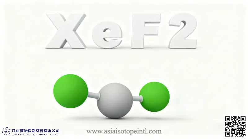
Xenon Difluoride is unique because it is a solid crystal at room temperature that sublimes directly into a gas. In a FIB system, a precursor crucible holds the solid XeF₂, and a fine needle injects the vapor specifically at the point where the ion beam hits the chip surface.
The Mechanism of Gas-Assisted Etching
The interaction between the Gallium ion beam, the XeF₂ gas, and the Silicon substrate is a symphony of physics and chemistry.
- Adsorption: XeF₂ molecules flow out of the nozzle and adsorb (stick) onto the surface of the chip.
- Activation: The high-energy Gallium ions strike the surface. This adds energy to the system, breaking the Xe-F bonds and creating defects in the silicon lattice.
- Reaction: The liberated Fluorine atoms react aggressively with the Silicon. The chemical equation is straightforward: 2𝑋𝑒𝐹2+𝑆𝑖→𝑆𝑖𝐹4(𝑔𝑎𝑠)+2𝑋𝑒(𝑔𝑎𝑠)
- Desorption (The Key to Cleanliness): The product of this reaction is Silicon Tetrafluoride (𝑆𝑖𝐹4), which is a volatile gas. Unlike the solid debris created by physical sputtering, 𝑆𝑖𝐹4 simply floats away into the vacuum pump.
The Result: The “Volatile” Advantage
Because the waste product is a gas, redeposition is virtually eliminated. The material doesn’t fall back into the hole; it evaporates. This allows engineers to dig extremely deep, vertical trenches with pristine sidewalls. Furthermore, the chemical reaction is much faster than physical knocking, increasing the material removal rate (etch yield) by a factor of 10 to 100 times.
3. High Selectivity: The Surgeon’s Precision
In circuit editing, the most terrifying moment is the “end-point”—the moment you break through the layer you are removing and hit the layer you want to connect to.
If you are digging through Silicon to reach a metal conductor, you need the process to stop exactly at the metal. If you overshoot by even 50 nanometers, you might cut the wire you intended to probe, ruining the chip.
XeF₂ offers extraordinary material selectivity.
- Silicon (Si): XeF₂ reacts spontaneously and vigorously with Silicon.
- Metals (Al, Cu): XeF₂ does not form volatile compounds with Aluminum or Copper at room temperature. It tends to form a thin, non-volatile fluoride layer (passivation) on these metals.
- Dielectrics (SiO₂): The reaction with high-quality Silicon Dioxide is very slow compared to Silicon.
The Expert Insight: When using XeF₂ in a FIB, the “Chemical Enhancement” factor for Silicon is massive. However, for Aluminum or Oxide, the chemical enhancement is low or non-existent. Therefore, when the beam cuts through the Silicon and hits the Metal, the etch rate suddenly drops dramatically. This natural “braking system” gives the operator the control needed to expose a buried circuit line without severing it.
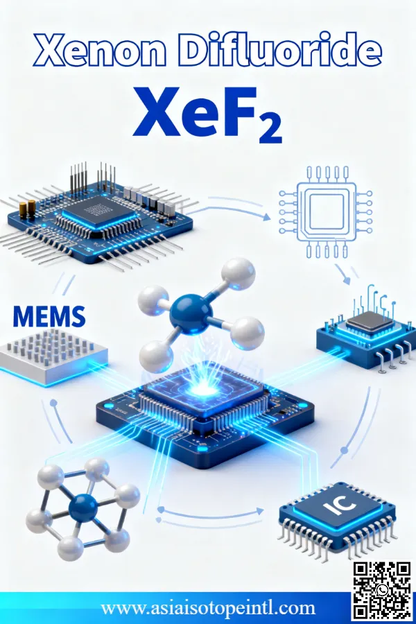
4. Primary Applications in Chip Repair and Debug
The utility of XeF₂ extends across several critical procedures in the failure analysis lab.
A. Backside Circuit Edit (The Flip-Chip Revolution)
Modern high-performance processors are packaged using “flip-chip” technology. The active circuitry is on the bottom, facing the package, while the top is covered by a massive heat sink. To edit these chips, engineers must go through the back—the bulk silicon substrate.
This substrate can be hundreds of microns thick.
- Without XeF₂: drilling through 100µm of silicon with just ions is practically impossible due to time and redeposition.
- With XeF₂: Engineers use the “Global Trencher” approach. XeF₂ is used to rapidly chemically excavate large “craters” in the silicon substrate (often 50µm x 50µm or larger). This removal is fast and clean, bringing the floor of the crater down to within a few microns of the active transistor layer. This is the single most common high-volume use of XeF₂ in Failure Analysis (FA) labs globally.
B. Molybdenum and Tungsten Removal
While Silicon is the primary target, XeF₂ is also highly effective for etching Tungsten (W) and Molybdenum (Mo). Tungsten is commonly used for “vias” (vertical connectors between layers) and contact plugs. When a circuit modification requires cutting a specific signal path, the engineer often needs to sever a Tungsten plug. XeF₂ facilitates this by forming Tungsten Hexafluoride (𝑊𝐹6), which, like 𝑆𝑖𝐹4, is a volatile gas. This allows for clean electrical isolation of circuit blocks.
C. Large Area Delayering
In Failure Analysis, sometimes the goal isn’t to fix the chip, but to find out why it failed. This requires stripping away layers to hunt for defects (like dust particles or short circuits). XeF₂ allows for the uniform removal of polysilicon layers or silicon substrates over large areas, exposing the fault location without introducing mechanical stress (which would happen if you used polishing pads).

5. Technical Nuances: Controlling the Isotropic Beast
As an expert, I must address a critical nuance: Spontaneity.
Unlike other FIB chemistries (like Chlorine or Iodine), XeF₂ reacts with Silicon spontaneously at room temperature, even without the ion beam. The ion beam greatly accelerates the reaction, but the background gas can still etch the silicon.
This creates a phenomenon known as Isotropic Etching or “undercutting.” If you are digging a square hole, the XeF₂ doesn’t just etch down; it etches sideways. It can tunnel underneath the protective oxide layers, creating a cave-like structure.
How we control it:
- Gas Flux Management: Skilled operators precisely control the needle position and gas pressure. Too much gas leads to excessive undercutting (the “wildfire” effect). Too little gas leads to redeposition (starvation regime).
- Beam Parameters: By using high beam currents and short pixel dwell times (the time the beam stays at one spot), we ensure the reaction is “mass transport limited”—meaning the reaction happens only where the beam is actively striking, minimizing lateral spread.
- Passivation Co-injection: In extremely advanced nodes (5nm), we sometimes co-inject other gases to passivate the sidewalls while XeF₂ etches the bottom, converting the isotropic etch into an anisotropic (directional) one.
This balance between the aggressive chemical nature of XeF₂ and the physical confinement of the ion beam is the art form of high-end circuit editing.
6. Comparison: XeF₂ vs. Other Halogens
Why is XeF₂ the industry standard? Why not generic Fluorine gas (𝐹2) or Chlorine (𝐶𝑙2)?
- Safety and Handling: 𝐹2 is terrifyingly reactive and dangerous to handle. Chlorine is corrosive and creates residual chlorides that can corrode the chip’s metal lines weeks after the repair is finished (the “time-bomb” effect).
- Stability: XeF₂ is a stable solid. It is easy to store in a small crucible attached to the microscope. It only releases fluorine when it sublimes and dissociates.
- Reaction Efficiency: The sticking coefficient (how well the molecule grabs onto the surface) of XeF₂ on Silicon is exceptionally high compared to other halogens.
- No Residue: The byproducts (𝑋𝑒 and 𝑆𝑖𝐹4) are chemically inert and leave no corrosive residues that could cause long-term reliability issues for the repaired chip.
7. The Economic Impact: Saving Millions
To appreciate the value of XeF₂, consider the economics of semiconductor design.
A “Mask Set” for a 5nm process node costs tens of millions of dollars. If a design team finds a logic bug (e.g., an AND gate should have been an OR gate) during the testing of the first prototype:
- Scenario A (No XeF₂/FIB): They must guess the fix, pay for a new mask set ($10M+), wait 3 months for fabrication, and pray it works.
- Scenario B (With XeF₂/FIB): They take the existing prototype chips to the lab. Using XeF₂-assisted FIB, they physically cut the connection to the AND gate and rewire it (using Platinum deposition) to create the OR logic. They test this “surgically altered” chip. If it works, they order the new masks with 100% confidence.
In this context, a few grams of XeF₂ enables a validation process that secures huge investments. It acts as the “Delete” and “Cut” key for hardware that is supposedly “hard.”
8. Future Trends: XeF₂ in the Angstrom Era
As we move toward Gate-All-Around (GAA) transistors and backside power delivery networks (BS-PDN), the role of XeF₂ is evolving.
- Extreme Aspect Ratios: Chips are getting thicker vertically (3D stacking). XeF₂ is the only known method capable of digging the ultra-deep trenches required to access signals in 3D-IC stacks without stalling due to redeposition.
- New Channel Materials: While Silicon is still king, Silicon-Germanium (SiGe) is common in high-speed circuits. XeF₂ etches SiGe even faster than Si, making it perfectly compatible with next-gen heterostructures.
- Atomic Layer Precision: Research is combining XeF₂ with pulsed electron beams (EBIE) rather than ion beams, allowing for damage-free etching that removes material layer by atomic layer, critical for quantum computing device fabrication.
Conclusion
In the grand machinery of the semiconductor industry, Xenon Difluoride is a silent workhorse. It is a material that embodies the perfect synergy of chemistry and physics. By transforming solid silicon into harmless vapor, it allows engineers to correct the mistakes of the past and verify the designs of the future.
For the failure analysis engineer, XeF₂ is not just a gas; it is the difference between a successful repair and a destroyed sample. As chips become more complex, the ability to perform precise, selective, and clean nanoscale excavation using this unique noble gas compound will remain a cornerstone of technological progress.
It turns the impossible task of rewiring a billion-transistor brain into a routine procedure.
Would you like a deeper dive into any specific technical parameters or applications?
As an industry leader focused in Specialty Gases products, our goal is to support our customers by keeping them at the forefront of their industries. We’re here to help with any questions you might have so you can transform your ideas into reality, and tackle those big science challenges.
Get free consultant, our experts are ready to serve.
(Follow up our update articles on www.asiaisotopeintl.com or send your comments to tao.hu@asiaisotope.com for further communications)