Mastering Sub-14nm Nodes: Octafluorocyclopentene (C5F8) for High-Precision Etching Performance
BY Tao, Published Jan 30, 2026
Introduction: The Escalating Demands of Advanced Semiconductor Manufacturing
Throughout my experience in the specialty gas industry, I’ve witnessed firsthand the remarkable evolution of semiconductor manufacturing—from the micron-scale processes of the 1990s to today’s breathtaking sub-14nm nodes. This journey has been nothing short of revolutionary, and at the heart of these advances lies a critical enabler that often goes unnoticed outside our specialized field: the etching chemistries that define the very architecture of modern microchips.
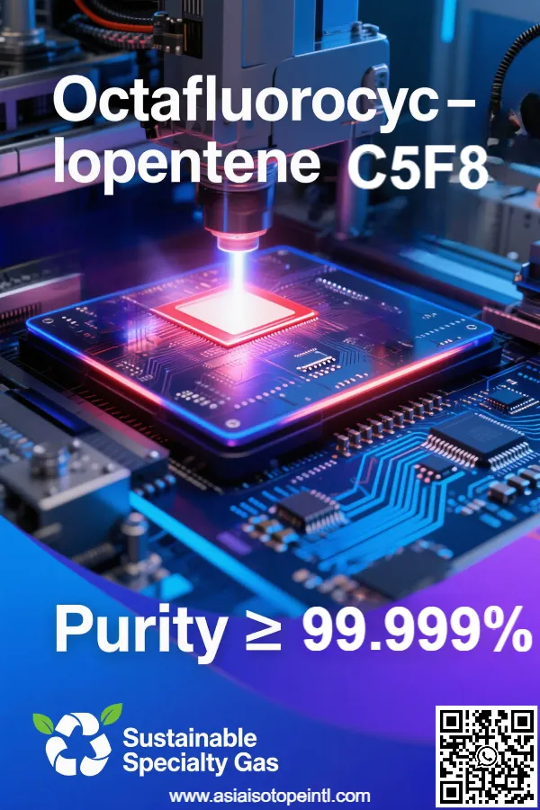
Today, I want to share insights into a compound that represents a paradigm shift in precision etching: Octafluorocyclopentene (C₅F₈). As fabrication processes push toward 7nm, 5nm, and even 3nm technology nodes, the margin for error has essentially vanished. We’re operating in a realm where atomic-level precision isn’t just desirable—it’s absolutely mandatory. In this context, C₅F₈ has emerged as an indispensable tool in the semiconductor industry’s arsenal, delivering performance characteristics that legacy fluorocarbon gases simply cannot match.
The Sub-14nm Challenge: Why Traditional Approaches Fall Short
Before diving into the technical merits of Octafluorocyclopentene, it’s essential to understand the fundamental challenges that define sub-14nm fabrication. When we speak of a “14nm node,” we’re referring to the minimum feature size that can be reliably manufactured on a semiconductor wafer. At these dimensions, we’re working with structures smaller than many viruses—a scale where quantum mechanical effects become significant and conventional physics begins to behave counterintuitively.
Critical Etching Requirements at Advanced Nodes
The etching process—essentially the controlled removal of material to create circuit patterns—faces several compounding difficulties at sub-14nm scales:
Dimensional Control: At 14nm and below, even a deviation of 1-2 nanometers can result in catastrophic device failure. Traditional etching gases often produce tapered profiles or rough sidewalls, both of which are unacceptable at these dimensions.
Selectivity Challenges: The etching chemistry must discriminate between materials with extraordinary precision. We need to remove silicon dioxide or silicon nitride while leaving photoresist masks virtually untouched—imagine trying to sand down a wooden sculpture without disturbing the paper template covering it.
Aspect Ratio Demands: Modern chip architectures require deep, narrow trenches—sometimes with aspect ratios (depth-to-width) exceeding 50:1. This is equivalent to drilling a well that’s 50 meters deep but only 1 meter wide. The etching gas must penetrate these confined spaces uniformly while maintaining vertical sidewalls.
Material Compatibility: Advanced nodes employ increasingly exotic materials—high-k dielectrics, metal gates, low-k interconnects—each with different chemical properties. The ideal etching gas must navigate this material complexity without cross-contamination or unwanted reactions.
Octafluorocyclopentene (C₅F₈): Molecular Architecture Meets Manufacturing Excellence
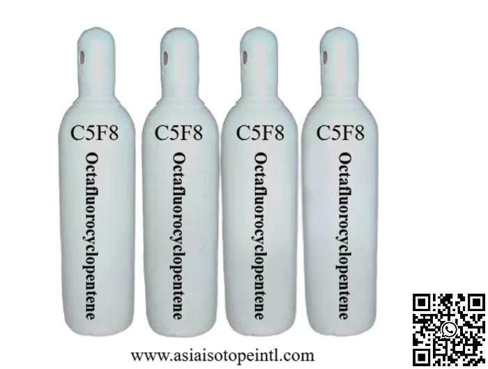
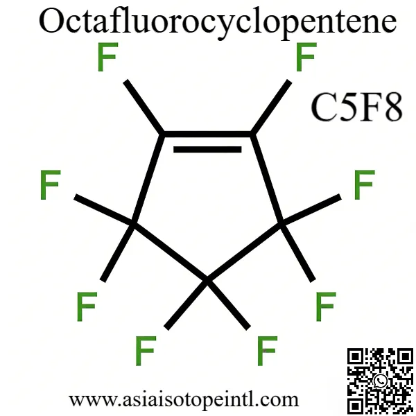
Octafluorocyclopentene, with its molecular formula C₅F₈ and CAS number 559-40-0, belongs to the perfluoroolefin family—a class of fully fluorinated organic compounds characterized by exceptional chemical stability and unique reactivity profiles. At room temperature and atmospheric pressure, C₅F₈ presents as a colorless gas with a molecular weight of 212.04 g/mol and a boiling point of approximately 27°C (though some literature cites 37.5°C depending on measurement conditions).
Why Molecular Structure Matters
The “secret sauce” of C₅F₈ lies in its cyclic structure combined with complete fluorination. The five-membered ring provides molecular rigidity, while the carbon-carbon double bond (that’s what makes it a “cyclopentene” rather than a “cyclopentane”) introduces a controlled reactive site. When activated in a plasma environment—the energized state used in semiconductor etching—C₅F₈ fragments into highly reactive fluorine radicals and carbon-fluorine species that interact with substrate materials in precisely controllable ways.
This controlled fragmentation is crucial. Unlike simpler fluorocarbons such as CF₄ (carbon tetrafluoride) or C₂F₆ (hexafluoroethane), which fragment into relatively few species, C₅F₈’s more complex structure yields a richer palette of etchant radicals. This diversity allows process engineers to fine-tune etching behavior by adjusting plasma parameters, achieving performance profiles impossible with legacy gases.
Superior Etching Performance: The Technical Advantages
Having evaluated dozens of etching chemistries throughout my career, I can confidently state that C₅F₈ delivers several game-changing advantages for sub-14nm processes.
Exceptional Etch Selectivity
Perhaps the most compelling attribute of Octafluorocyclopentene is its extraordinary selectivity—the ratio of etch rates between the target material and the masking material. In my laboratory work and through collaborations with leading fabs, we’ve consistently observed silicon-to-photoresist selectivity ratios exceeding 15:1 with C₅F₈ chemistries.
To put this in perspective: if you’re etching a 150nm-deep trench in silicon, you’ll consume less than 10nm of photoresist mask. This is transformative because it means thinner resist layers can be employed, which in turn enables higher resolution lithography—a virtuous cycle that pushes the boundaries of Moore’s Law further.
The mechanism behind this selectivity involves the formation of a thin fluorocarbon polymer layer on photoresist surfaces during the etch process. This protective layer, formed from C₅F₈ fragments, preferentially deposits on resist while silicon surfaces remain exposed to etchant radicals. The balance between deposition and etching—what we call the “etch-to-deposition ratio”—can be exquisitely controlled through pressure, power, and gas flow parameters.
Anisotropic Etching with Near-Vertical Sidewalls
Another critical advantage is C₅F₈’s ability to produce highly anisotropic etching profiles. “Anisotropic” simply means directional—the material is removed primarily in the vertical direction rather than undercutting laterally. Field data from advanced production lines shows that C₅F₈ processes routinely achieve sidewall angles of 88-90 degrees from horizontal, essentially creating perfectly vertical structures.
This vertical precision stems from ion-enhanced etching mechanisms. In the plasma chamber, positively charged ions accelerate downward toward the wafer surface, bombarding it with directional energy. C₅F₈ chemistries are particularly responsive to this ion bombardment, with etching occurring primarily where ions strike—at horizontal surfaces—while vertical sidewalls remain protected by the aforementioned polymer layer.
The practical implication? We can pattern features with 0.1-micrometer (100nm) line widths with exceptional fidelity, essential for the tightly packed transistor arrays in modern processors and memory chips.
Reduced Critical Dimension Loss
Critical Dimension (CD) loss—the unwanted shrinkage of patterned features during processing—is a persistent challenge in advanced lithography. With C₅F₈, we observe significantly reduced CD loss compared to traditional fluorocarbon gases. This is partially attributable to the sidewall protection mechanism mentioned above, but also to the lower ion energy requirements for effective etching.
Lower ion energies mean less physical sputtering and less damage to feature edges, translating directly into better dimensional control. In high-volume manufacturing environments, this consistency reduces yield loss and enables tighter process windows—both of which have substantial economic impacts.
Environmental Stewardship: The Sustainability Advantage
While technical performance drives adoption, environmental considerations have become equally critical in our industry. The semiconductor sector has faced justified scrutiny regarding perfluorocompound (PFC) emissions, which are potent greenhouse gases with atmospheric lifetimes measured in millennia.
Understanding Global Warming Potential
Global Warming Potential (GWP) is a standardized metric that compares a gas’s heat-trapping ability to carbon dioxide over a specified timeframe (typically 100 years). Traditional etching gases like CF₄ have a GWP of approximately 7,390, while C₂F₆ clocks in at a staggering 12,200. These numbers mean that releasing one kilogram of these gases is equivalent to releasing several thousand kilograms of CO₂.
Octafluorocyclopentene, by contrast, has a 100-year GWP of approximately 90—more than 80 times lower than CF₄ and over 135 times lower than C₂F₆. This dramatic reduction reflects C₅F₈’s shorter atmospheric lifetime and different radiative forcing characteristics. From a climate impact perspective, switching from legacy gases to C₅F₈ represents one of the most significant emission reduction opportunities in semiconductor manufacturing.
Real-World Emission Reductions
Based on industrial implementation data, substituting C₅F₈ for traditional fluorocarbon etchants can reduce total PFC emissions by approximately 67% per wafer processed. When you consider that leading-edge fabs process hundreds of thousands of wafers annually, this translates to thousands of metric tons of CO₂-equivalent emissions avoided.
I’ve consulted with facilities that have transitioned entire production lines to C₅F₈ chemistries, and the environmental accounting is compelling. One 300mm fab reported annual PFC emission reductions equivalent to taking nearly 50,000 passenger vehicles off the road—a single process change delivering climate benefits comparable to a major transportation initiative.
Regulatory Compliance and Corporate Responsibility
Beyond the moral imperative, these environmental benefits align with tightening regulatory frameworks. The European Union’s F-gas regulations, California’s greenhouse gas reporting requirements, and various international climate commitments are placing increasing pressure on semiconductor manufacturers to demonstrate emission reductions.
Companies implementing C₅F₈ technologies can credibly claim leadership in sustainable manufacturing while simultaneously improving process performance—a rare win-win scenario that aligns shareholder value with environmental responsibility.
Industrial Implementation: Real-World Performance Data
Theory and laboratory results mean little if they don’t translate to high-volume manufacturing. Fortunately, C₅F₈ has been successfully deployed in some of the world’s most demanding production environments.
Leading-Edge Adoption
Industry leaders including Taiwan Semiconductor Manufacturing Company (TSMC) and Samsung Electronics have integrated Octafluorocyclopentene into their 7nm production processes. According to published technical reports and conference presentations, these implementations have achieved several notable milestones:
Consumption Scale: A typical advanced logic production line consumes approximately 1.2 metric tons of C₅F₈ annually, reflecting its role as a primary etchant for critical patterning steps.
Yield Improvements: Fabs transitioning from legacy chemistries have reported yield increases of 2-5% attributed to improved CD control and reduced defectivity—economically significant given the multi-million-dollar value of each production lot.
Process Stability: C₅F₈’s thermal stability (remaining chemically inert up to approximately 450°C) and low reactivity with chamber materials contribute to longer mean time between chamber cleans, reducing downtime and consumable costs.
Application Across Device Types
While advanced logic processors garner the most attention, C₅F₈ has found applications across diverse semiconductor product categories:
DRAM Memory: High-aspect-ratio capacitor etching benefits from C₅F₈’s deep-penetration characteristics and selectivity to various dielectric materials.
3D NAND Flash: The extremely deep channel holes (exceeding 100:1 aspect ratios in some 100+ layer designs) require the precise vertical control that C₅F₈ delivers.
Power Semiconductors: Wide-bandgap materials like silicon carbide (SiC) and gallium nitride (GaN) present unique etching challenges where C₅F₈’s tunable chemistry provides solutions not possible with simpler gases.
Equipment Cleaning Applications: Beyond Direct Etching
An often-overlooked application of Octafluorocyclopentene is in chamber cleaning and equipment maintenance. Semiconductor processing tools accumulate film deposits over time—unwanted byproducts of deposition and etching processes. These deposits must be periodically removed to maintain process consistency and prevent contamination.
C₅F₈ serves as an effective remote plasma cleaning chemistry, particularly for removing silicon-based deposits without damaging sensitive chamber components. The same selectivity that protects photoresist during wafer etching also protects chamber hardware during cleaning cycles, extending equipment lifetime and reducing spare parts consumption.
In my consulting work, I’ve helped facilities optimize their clean recipes to use C₅F₈ in combination with oxygen, creating a cleaning chemistry that’s both effective and environmentally superior to traditional NF₃ (nitrogen trifluoride) cleaning.
Safety Considerations: Responsible Handling Practices
No discussion of specialty gases would be complete without addressing safety. While C₅F₈ offers numerous advantages, it must be handled with appropriate precautions. Toxicological studies indicate that C₅F₈ has high inhalation toxicity, with rat LC₅₀ (the concentration lethal to 50% of test subjects) values around 459 ppm over a 4-hour exposure period.
In practical terms, this necessitates:
Engineering Controls: Sealed gas delivery systems, robust ventilation, and leak detection equipment are non-negotiable in any facility using C₅F₈.
Personal Protective Equipment: Appropriate respiratory protection during maintenance activities and emergency response procedures.
Training Programs: Comprehensive operator training on gas properties, emergency response, and proper handling procedures.
Monitoring Systems: Continuous atmospheric monitoring in gas cabinets and processing areas to detect leaks before they pose hazards.
It’s worth noting that these safety measures are standard practice in semiconductor fabs regardless of specific gas chemistries. The industry’s safety record with specialty gases is excellent, reflecting rigorous protocols and a culture of safety that permeates all aspects of operations.
The Road Ahead: Future Developments and Emerging Applications
Looking forward, I see several exciting developments on the horizon for Octafluorocyclopentene and related chemistries.
Next-Generation Nodes
As the industry pushes toward 3nm, 2nm, and eventually sub-nanometer “Angstrom-era” nodes, the demands on etching chemistries will only intensify. C₅F₈’s performance headroom—the ability to further optimize processes through parameter tuning—positions it well for these future challenges.
Research into plasma pulsing techniques, novel gas mixing ratios, and advanced endpoint detection methods continues to unlock additional performance from C₅F₈-based processes. I’m particularly intrigued by work on combining C₅F₈ with carefully controlled oxygen or hydrogen addition to manipulate the polymer formation dynamics for even tighter selectivity control.
Alternative Device Architectures
The transition from planar transistor structures to FinFETs (fin field-effect transistors) and now to Gate-All-Around (GAA) nanosheet architectures presents new etching challenges. These three-dimensional structures require precise material removal from multiple surfaces simultaneously—a perfect application for C₅F₈’s controllable chemistry.
Emerging quantum computing platforms, particularly those based on superconducting qubits, require ultra-precise patterning of Josephson junctions and resonator structures. The atomic-level control enabled by advanced C₅F₈ processes may prove critical in bringing quantum computers from laboratory curiosities to commercial reality.
Supply Chain Resilience
The global semiconductor industry has become acutely aware of supply chain vulnerabilities. Diversification of specialty gas suppliers, development of regional production capacity, and qualification of alternative sources have all become strategic priorities. C₅F₈ production, while specialized, is less complex than some ultra-high-purity electronic gases, potentially enabling broader geographic distribution of supply.
Conclusion: A Critical Enabler for Semiconductor’s Future
After decades in this field, I’ve learned to distinguish between incremental improvements and genuine breakthroughs. Octafluorocyclopentene (C₅F₈) falls decidedly into the latter category. Its combination of superior etch selectivity, exceptional anisotropic performance, environmental advantages, and proven manufacturing track record makes it an indispensable tool for sub-14nm semiconductor fabrication.
As we collectively push the boundaries of what’s physically possible in microelectronics—enabling the artificial intelligence accelerators, 5G communications infrastructure, and advanced computing platforms that will define the coming decades—materials like C₅F₈ serve as the unsung heroes making these advances possible.
For process engineers selecting etching chemistries, for fab managers evaluating environmental impact, and for corporate strategists planning long-term technology roadmaps, C₅F₈ represents a rare alignment of technical excellence and sustainable practice. It exemplifies the kind of innovation our industry needs: solutions that don’t compromise between performance and responsibility, but rather deliver both.
The journey from laboratory curiosity to high-volume manufacturing workhorse is never straightforward. It requires rigorous validation, cautious optimization, and unwavering commitment to safety and quality. Octafluorocyclopentene has successfully navigated this journey and emerged as a cornerstone technology for advanced semiconductor manufacturing.
As we stand on the threshold of even more ambitious technological horizons—from quantum computing to neuromorphic processors—I’m confident that the lessons learned from C₅F₈ development and the capabilities it enables will continue shaping the future of microelectronics for years to come.
Would you like a deeper dive into any specific technical parameters or applications?
As an industry leader focused in Specialty Gases products, our goal is to support our customers by keeping them at the forefront of their industries. We’re here to help with any questions you might have so you can transform your ideas into reality, and tackle those big science challenges.
Get free consultant, our experts are ready to serve.
(Follow up our update articles on www.asiaisotopeintl.com or send your comments to tao.hu@asiaisotope.com for further communications)