Description
Product Name: Octafluorocyclopentene C5F8 / Perfluorocyclopentene
CAS: 559-40-0
Purity: 4N ~5N
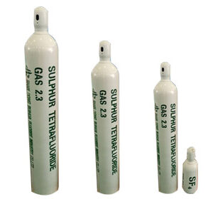
Product specifications: 4L/8L/10L
Product form: Octafluorocyclopentene C5F8 / Perfluorocyclopentene
Main use: Plasma etching process.
Availability : Pre Stock (Customized manufacturing )
What is Octafluorocyclopentene (C5F8) ?
Octafluorocyclopentene (C5F8) is a toxic, non-flammable, low boiling point (81 °F) colorless liquified gas with a slight distinctive odor. Octafluorocyclopentene (C5F8) is mainly used in Plasma Etching Process , especially in Advanced Process Etching of14nm and below process nodes, which is suitable for precise etching of high aspect ratio structures (such as FinFET, 3D NAND memory cells).
Certificate of Analysis
| Component | Unit | Specification |
| C5F8 | % | ≥99.99 |
| C4F6 | ppm | ≤ 50 |
| O2 + Ar | ppm | ≤ 20 |
| N2 | ppm | ≤ 100 |
| H2O | ppm | ≤ 10 |
NOTE : For grade 99.999% don’t hesitate to call or contact tao.hu@asiaisotope.com for more technical details.
What are applications of Octafluorocyclopentene (C5F8) ?
Octafluorocyclopentene (C5F8) is a toxic, non-flammable, low boiling point (81 °F) colorless liquified gas with a slight distinctive odor. Octafluorocyclopentene (C5F8) is mainly used in Plasma Etching Process , especially in Advanced Process Etching of14nm and below process nodes, which is suitable for precise etching of high aspect ratio structures (such as FinFET, 3D NAND memory cells).
1. Plasma Etching Process (Main Application)
- Advanced Process Etching: 14nm and below process nodes, especially suitable for precise etching of high aspect ratio structures (such as FinFET, 3D NAND memory cells)
- Pattern Transfer: Achieving precise replication of nanoscale patterns on materials such as silicon, silicon dioxide, and silicon nitride
- Dry Etching: As a plasma etching gas, it combines physical bombardment and chemical reaction to achieve anisotropic etching.
2. Semiconductor Equipment Cleaning
- Cavity Cleaning: Used for removing chamber residues after CVD/PECVD, replacing traditional PFC cleaning gases and reducing greenhouse gas emissions by more than 95%.
- Pipeline Cleaning: Suitable for precision cleaning of semiconductor process pipelines to prevent cross-contamination.
| Application Scenarios | Advantages | Technical Specifications |
|---|---|---|
| FinFET Structure Etching | Precisely control fin width and verticality, preventing sidewall erosion | Sidewall angle: 88°, line width control precision: 0.1μm level |
| 3D NAND High Aspect Ratio Holes/Grooves | High selectivity, reducing photoresist consumption and improving yield | Silicon/photoresist selectivity: ≥15:1, aspect ratio: >30:1 |
| DRAM Capacitor Structure | Reduce residues and enhance structural stability | Etching uniformity: >98%, residues: <0.01ppm |
| Advanced Interconnect Structure | Precisely control via and trench profiles, reducing RC delay | Critical dimension (CD) control precision: <5nm |
* * * Can’t Find What You Are Looking For ? Contact Us tao.hu@asiaisotope.com As We Still Might Be Able To Make It * * *