Xenon Gas in Advanced Semiconductor Manufacturing: Why Plasma Etching with Xe Defines Next-Generation Chip Fabrication
BY Tao, Published Feb 1, 2026
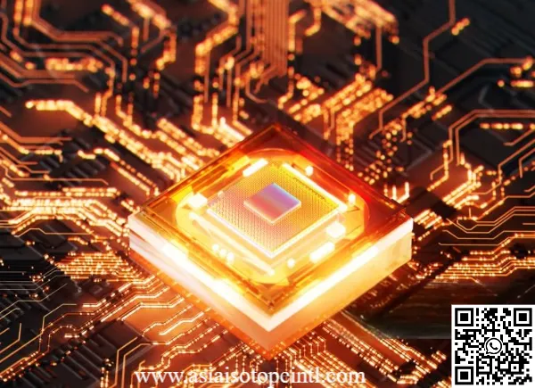
In the relentless pursuit of smaller, faster, and more powerful microchips, the semiconductor industry has pushed the boundaries of physics and chemistry to extraordinary limits. Today’s most advanced processors contain billions of transistors, each smaller than a virus, arranged in three-dimensional architectures of breathtaking complexity. Behind this technological marvel lies an unsung hero: Xenon (Xe)—a rare noble gas that has become indispensable in defining the nanoscale features of next-generation chips.
As China Isotope Development Co Ltd was supplying ultra-high-purity gases to the world’s leading chip manufacturers, I have witnessed firsthand how Xenon has evolved from a niche laboratory curiosity to a critical enabler of modern semiconductor fabrication. In this comprehensive article, I will explain the science behind Xenon-based plasma etching, explore its unique advantages over alternative gases, and demonstrate why this heavy noble gas is shaping the future of chip manufacturing.
1. The Semiconductor Challenge: Why Etching Matters
To understand Xenon’s role, we must first appreciate the fundamental challenge of chip manufacturing: pattern transfer.
From Design to Silicon
A microchip begins as a design—a digital blueprint containing billions of geometric shapes representing transistors, interconnects, and other components. The challenge is transferring this design onto a physical silicon wafer with nanometer-level precision.
This is accomplished through a series of deposition and etching steps:
- Deposition: Thin films of various materials (silicon, silicon dioxide, metals, etc.) are layered onto the wafer.
- Lithography: A light-sensitive coating (photoresist) is applied and exposed to patterned light, creating a mask.
- Etching: Material is selectively removed from areas not protected by the mask, transferring the pattern into the underlying film.
Etching is where Xenon enters the picture. The precision, selectivity, and cleanliness of the etching process directly determine the quality and performance of the final chip.
The Evolution of Etching Technology
Early semiconductor manufacturing relied on wet etching—immersing wafers in liquid chemicals that dissolved exposed material. While simple, wet etching is isotropic, meaning it removes material equally in all directions. This creates undercut profiles unsuitable for the fine features required in modern chips.
The industry transitioned to dry etching or plasma etching, which uses ionized gases (plasma) to remove material. Plasma etching can be highly anisotropic (directional), enabling the vertical sidewalls essential for dense, high-performance circuits.
2. Plasma Etching Fundamentals: The Physics of Precision
Before diving into Xenon’s specific applications, let me explain how plasma etching works.
What is Plasma?
Plasma is often called the “fourth state of matter.” When a gas is energized sufficiently (through heat, electromagnetic fields, or electrical discharge), its atoms lose electrons, creating a soup of positive ions, free electrons, and neutral atoms. This electrically conductive, highly reactive state is plasma.
The Etching Mechanism
In a plasma etching chamber:
- Process gases are introduced at low pressure (typically millitorr to torr range).
- Radio frequency (RF) or microwave energy ionizes the gas, creating plasma.
- Reactive species (ions, radicals, neutral atoms) interact with the wafer surface.
- Material is removed through chemical reactions (reactive ion etching), physical bombardment (ion beam etching), or a combination of both.
The beauty of plasma etching lies in its tunability. By adjusting gas composition, pressure, power, and bias voltage, engineers can precisely control etch rate, selectivity (etching one material while preserving another), and profile shape.
3. Xenon‘s Unique Atomic Properties: The Foundation of Excellence
Why Xenon? Among all the elements available to semiconductor engineers, Xenon possesses a remarkable combination of properties that make it exceptionally valuable for specific etching applications.
High Atomic Mass
Xenon has an atomic mass of 131.3 atomic mass units (u)—the heaviest stable noble gas. This mass is crucial for physical sputtering processes, where momentum transfer determines material removal efficiency.
When a heavy Xenon ion strikes a surface, it transfers significant kinetic energy. This enables efficient removal of stubborn materials that resist chemical attack, such as certain metals and compound semiconductors.
Chemical Inertness
As a noble gas, Xenon has a complete outer electron shell, making it extraordinarily unreactive under normal conditions. This inertness is a double-edged sword:
- Advantage: Xenon plasma causes minimal chemical damage to sensitive structures.
- Opportunity: Under specific conditions, Xenon can form compounds (like XeF₂) that offer unique etching chemistries.
Low Ionization Energy
Xenon has a relatively low first ionization energy (12.13 eV), meaning it readily forms ions when exposed to plasma conditions. This translates to efficient plasma generation and stable process conditions—critical for manufacturing repeatability.
Large Atomic Radius
Xenon’s large atomic radius (216 pm) affects its interaction with surfaces and its behavior in plasma. The size contributes to its effectiveness in certain sputtering and ion implantation applications.
4. XeF₂: The Revolutionary Etching Chemistry
Perhaps the most significant application of Xenon in semiconductor manufacturing involves not pure Xenon, but its compound: Xenon Difluoride (XeF₂).
A Noble Gas That Reacts
XeF₂ is one of the few stable compounds of a noble gas. It exists as a white crystalline solid at room temperature, subliming (converting directly to gas) at low pressures. This seemingly simple molecule has revolutionized certain semiconductor processes.
The XeF₂ Etching Mechanism
When XeF₂ vapor contacts silicon at room temperature, a remarkable spontaneous reaction occurs:
2XeF₂ + Si → 2Xe + SiF₄
The fluorine atoms from XeF₂ attack silicon, forming volatile silicon tetrafluoride (SiF₄) that is pumped away. The Xenon is released as an inert byproduct.
This reaction is:
- Highly selective: XeF₂ etches silicon rapidly but barely affects silicon dioxide, silicon nitride, aluminum, and photoresist.
- Isotropic: The etch proceeds equally in all directions, creating rounded, undercut profiles.
- Gentle: No plasma is required; the reaction occurs at low temperatures without ion bombardment damage.
MEMS: Where XeF₂ Shines
Microelectromechanical Systems (MEMS) are miniature mechanical devices—accelerometers, pressure sensors, microphones, gyroscopes—fabricated using semiconductor techniques. MEMS are found in smartphones, automobiles, medical devices, and industrial equipment.
Many MEMS devices require release etching—the removal of a sacrificial silicon layer to free mechanical structures (beams, membranes, cantilevers) so they can move.
XeF₂ is the gold standard for MEMS release etching because:
- Stiction Prevention: Wet etching can cause delicate structures to stick together due to surface tension as the liquid dries. XeF₂ is a dry, vapor-phase process that eliminates this problem.
- Selectivity: XeF₂ removes silicon without attacking the silicon dioxide or metal structures common in MEMS.
- Gentle Processing: No plasma damage means fragile mechanical structures remain intact.
- Penetration: The gaseous nature allows XeF₂ to reach deeply buried sacrificial layers through small access holes.
Leading MEMS manufacturers—producing components for Apple, Samsung, automotive suppliers, and medical device companies—rely on XeF₂ etching as an irreplaceable process step.
5. Xenon in Ion Beam Etching and Milling
Beyond XeF₂ chemistry, pure Xenon plays a critical role in Ion Beam Etching (IBE) and Ion Beam Milling—physical processes that use accelerated ions to sputter material from surfaces.
How Ion Beam Etching Works
In IBE:
- Xenon gas is introduced into an ion source chamber.
- Electrons ionize the Xenon, creating Xe⁺ ions.
- The ions are extracted and accelerated through grids to energies of 200-2000 eV.
- The collimated ion beam strikes the wafer at a controlled angle.
- Momentum transfer ejects (sputters) atoms from the surface.
Why Xenon for Ion Beams?
Xenon’s heavy mass makes it exceptionally effective for physical sputtering:
| Ion Species | Atomic Mass (u) | Relative Sputter Yield |
|---|---|---|
| Argon (Ar) | 40 | 1.0 (baseline) |
| Krypton (Kr) | 84 | ~1.3 |
| Xenon (Xe) | 131 | ~1.5-1.8 |
Xenon ions deliver approximately 50-80% higher sputter yields than Argon for many materials. This means faster processing and higher throughput.
Applications of Xenon Ion Beam Etching
1. Magnetic Thin Film Patterning The magnetic read/write heads in hard disk drives and the magnetic tunnel junctions in MRAM (Magnetoresistive Random Access Memory) require precise patterning of complex multilayer metal stacks. These materials often cannot be etched chemically. Xenon IBE provides the physical removal mechanism needed while minimizing damage to sensitive magnetic properties.
2. Compound Semiconductor Processing Materials like Gallium Arsenide (GaAs), Indium Phosphide (InP), and Gallium Nitride (GaN)—used in RF devices, LEDs, and power electronics—are difficult to etch with conventional fluorine or chlorine chemistries. Xenon ion milling offers a universal physical etching solution.
3. Trimming and Repair Xenon Focused Ion Beam (FIB) systems are used for:
- Circuit editing and repair
- Failure analysis (cross-sectioning chips to examine internal structures)
- Photomask repair
- TEM (Transmission Electron Microscopy) sample preparation
The heavy Xenon ions mill material efficiently while the inert nature minimizes unwanted implantation effects compared to the traditionally used Gallium FIB.
6. Xenon in Advanced Plasma Processes
High-Density Plasma Applications
In certain high-density plasma reactors, Xenon serves as a buffer gas or carrier gas, providing:
- Plasma stabilization: Xenon’s ionization characteristics help maintain stable plasma conditions.
- Energy transfer: Xenon atoms can absorb and redistribute energy within the plasma, moderating electron temperatures.
- Dilution: Adding Xenon to reactive gas mixtures allows fine-tuning of etch rates and selectivity.
Atomic Layer Etching (ALE)
As the industry pushes toward sub-5nm technology nodes, Atomic Layer Etching—removing material one atomic layer at a time—becomes essential. Some ALE processes utilize Xenon or Xenon-containing plasmas for the physical removal step, leveraging the precise momentum transfer of heavy Xe ions to desorb surface species without damaging underlying layers.
7. The Technical Advantages: Xenon vs. Alternative Gases
Let me summarize why Xenon outperforms alternatives in specific semiconductor applications:
Xenon vs. Argon in Ion Beam Processes
| Parameter | Argon | Xenon | Advantage |
|---|---|---|---|
| Atomic Mass | 40 u | 131 u | Xe: Higher sputter yield |
| Sputter Efficiency | Baseline | +50-80% | Xe: Faster processing |
| Implantation Depth | Deeper | Shallower | Xe: Less subsurface damage |
| Cost | Lower | Higher | Ar: Economics |
For critical applications where performance trumps cost, Xenon is the clear winner.
XeF₂ vs. SF₆ Plasma for Silicon Etching
| Parameter | SF₆ Plasma | XeF₂ Vapor |
|---|---|---|
| Plasma Required | Yes | No |
| Ion Bombardment | Yes | No |
| Selectivity to SiO₂ | Moderate | Excellent (>1000:1) |
| Stiction Risk | Lower | None |
| Profile | Anisotropic possible | Isotropic only |
| Damage to Structures | Moderate | Minimal |
For MEMS release and sensitive structures, XeF₂ is irreplaceable.
8. Applications in Next-Generation Chip Fabrication
The semiconductor roadmap demands ever-smaller features, three-dimensional architectures, and novel materials. Xenon-based processes address several critical challenges:
3D NAND Flash Memory
Modern flash memory stacks dozens or even hundreds of memory cell layers vertically. Creating the deep, high-aspect-ratio holes and trenches through these stacks requires sophisticated etching.
While the primary etch chemistries are fluorocarbon-based, Xenon-containing gas mixtures can:
- Improve etch profile control
- Reduce micromasking and defects
- Enhance selectivity to hard mask materials
FinFET and Gate-All-Around (GAA) Transistors
Advanced logic chips use 3D transistor architectures where the gate wraps around the channel. Fabricating these structures requires atomic-precision etching with minimal damage.
Xenon ion beam trimming and ALE processes enable:
- Precise fin width control
- Smooth sidewall surfaces
- Removal of damaged layers after aggressive etching
Advanced Packaging
Modern chips increasingly use heterogeneous integration—combining multiple chiplets in a single package. This requires:
- Through-Silicon Vias (TSVs) for vertical interconnection
- Precise trench etching for embedded components
- MEMS-like release processes for certain packaging structures
XeF₂ and Xenon plasma processes play enabling roles in these advanced packaging technologies.
Emerging Memory Technologies
Next-generation memories—MRAM, ReRAM, PCRAM—use exotic materials (magnetic alloys, metal oxides, chalcogenides) that require careful physical etching. Xenon ion beam processes are often the only viable option for patterning these materials without degrading their functional properties.
9. Purity Requirements: The Expert’s Perspective
As a specialty gas supplier, I must emphasize that semiconductor-grade Xenon must meet stringent purity specifications.
Contamination Concerns
In semiconductor manufacturing, contamination at parts-per-billion (ppb) levels can cause:
- Particle defects
- Film quality degradation
- Electrical failures
- Yield loss worth millions of dollars
Purity Specifications for Semiconductor Xenon
| Parameter | Typical Specification |
|---|---|
| Purity | ≥99.999% (5N) to 99.9999% (6N) |
| Oxygen (O₂) | <0.5 ppm |
| Moisture (H₂O) | <0.5 ppm |
| Nitrogen (N₂) | <2 ppm |
| Hydrocarbons | <0.1 ppm |
| Carbon Dioxide (CO₂) | <0.5 ppm |
| Krypton (Kr) | <5 ppm |
| Particles | <1 particle/ft³ (>0.1µm) |
XeF₂ Purity Considerations
For XeF₂, purity is equally critical. The compound must be free of:
- Moisture (which causes decomposition)
- HF (hydrofluoric acid, a dangerous contaminant)
- Particulates
- Other xenon fluorides (XeF₄, XeF₆)
Proper storage, handling, and delivery systems are essential. XeF₂ is typically stored in specially designed sublimation vessels and delivered through heated, passivated stainless steel lines.
10. Supply Chain and Market Considerations
Xenon Production and Scarcity
Xenon is extracted from air through cryogenic distillation, but its atmospheric concentration is minuscule—only 0.087 ppm (87 parts per billion). Global production is limited to approximately 40-60 metric tons annually.
The semiconductor industry competes for this limited supply with:
- Aerospace (ion propulsion)
- Medical (anesthesia, imaging)
- Lighting
- Research
Strategic Implications
For semiconductor fabs, Xenon supply security is a strategic concern. Major manufacturers:
- Establish long-term supply agreements
- Qualify multiple suppliers
- Maintain buffer inventories
- Invest in recycling and recovery systems
Cost-Benefit Analysis
While Xenon is expensive (often $1,000-2,000/kg for high-purity grades), the cost per wafer is manageable because:
- Xenon-based processes use relatively small quantities
- The value added by Xenon processes is enormous
- No alternatives exist for certain critical applications
A MEMS fab might consume only a few kilograms of XeF₂ per month, yet this enables production of millions of sensors worth hundreds of millions of dollars.
11. The Future: Emerging Trends and Innovations
Looking ahead, I see several developments that will expand Xenon’s role in semiconductor manufacturing:
Plasma-Enhanced XeF₂
Researchers are developing hybrid processes that combine XeF₂ chemistry with gentle plasma activation. This could enable:
- Higher etch rates
- Improved anisotropy
- New applications beyond MEMS
Cryogenic Etching with Xenon
Cryogenic etching (processing at very low temperatures) can dramatically improve etch profiles and selectivity. Xenon’s thermodynamic properties make it suitable for certain cryogenic plasma processes.
Xenon in EUV Lithography
Extreme Ultraviolet (EUV) lithography—the technology enabling sub-7nm chip production—uses plasma sources that may involve Xenon. While the primary EUV source uses Tin, Xenon plays roles in certain plasma diagnostic and conditioning processes.
Advanced Recycling Technologies
Given Xenon’s scarcity, the industry is developing sophisticated recycling systems that capture, purify, and reuse Xenon from exhaust streams. Recovery rates exceeding 90% are achievable, improving both economics and supply security.
12. Conclusion: The Indispensable Element
In the invisible world of semiconductor fabrication—where features are measured in atoms and success is defined by billions of perfect transistors—Xenon has earned its place as an indispensable specialty gas.
Its unique combination of high atomic mass, chemical versatility (both as inert Xe and reactive XeF₂), favorable ionization properties, and plasma compatibility makes it irreplaceable for:
- MEMS release etching with XeF₂
- Ion beam etching of magnetic and compound semiconductor materials
- Focused ion beam processing for analysis and repair
- Advanced plasma processes in next-generation chip fabrication
As the semiconductor industry continues its relentless march toward smaller, faster, and more complex devices, Xenon will remain at the heart of the fabrication toolbox. Its role may be invisible to the billions of people who use smartphones, computers, and countless other electronic devices daily, but without this rare noble gas, the digital age as we know it would not be possible.
From my perspective as a specialty gas expert who has spent a career at the intersection of chemistry and high technology, Xenon exemplifies how fundamental science enables transformative engineering. It is not merely a process gas—it is an enabling element of human progress.
Would you like a deeper dive into any specific technical parameters or applications?
As an industry leader focused in Specialty Gases products, our goal is to support our customers by keeping them at the forefront of their industries. We’re here to help with any questions you might have so you can transform your ideas into reality, and tackle those big science challenges.
Get free consultant, our experts are ready to serve.
(Follow up our update articles on www.asiaisotopeintl.com or send your comments to tao.hu@asiaisotope.com for further communications)