Advanced Xenon Difluoride Applications: From MEMS Device Release to IC Failure Analysis
BY Tao, Published Jan 3, 2026
Introduction: A “Small” Gas with outsized impact
In the world of semiconductor and MEMS manufacturing, the tools that really change the game are often not the ones that make headlines. One of the best examples is xenon difluoride (XeF₂) – a white crystalline solid that, when turned into vapor, becomes an extremely selective, room‑temperature etchant for silicon.
Originally seen as a chemical curiosity – one of the first stable noble‑gas compounds – XeF₂ has quietly evolved into a strategic process gas. It underpins high‑yield MEMS device release, enables delicate micro‑ and nano‑structures that wet chemistry would simply destroy, and has become a powerful ally in IC failure analysis and circuit debug.
What makes XeF₂ so valuable is the rare combination of:
- Plasma‑free, room‑temperature operation
- Highly isotropic etching of silicon
- Extraordinary selectivity over oxides, nitrides, metals and polymers
Those three features, together, open up process windows that are very hard – or outright impossible – to reach with conventional wet etch or plasma etch.
Over the past 3 years, China Isotope Development Co Ltd was starting to supply Xenon Difluoride (XeF₂) to China domestic clients. As a specialty‑gas and process engineer, how XeF₂ works, why it’s so selective, and how advanced fabs and labs are using it today – from state‑of‑the‑art MEMS device release to precision IC failure analysis and beyond.
1. What Makes Xenon Difluoride (XeF₂) Special?
1.1 Basic chemistry and structure
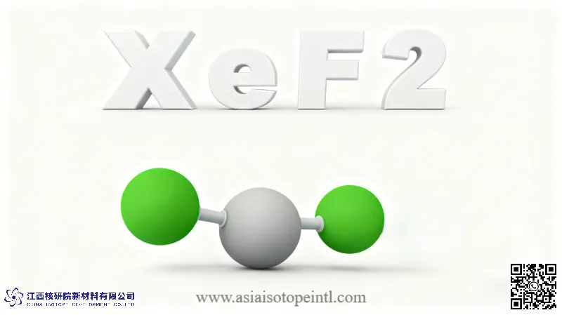
Xenon difluoride is an inorganic compound formed from xenon (a noble gas) and fluorine. At room temperature it is a colorless to white crystalline solid that sublimes readily – in other words, it turns directly from solid into vapor under vacuum or mild heating. https://en.wikipedia.org/wiki/Xenon_difluoride
The molecule is linear (F–Xe–F). Xenon adopts an expanded valence shell (often described as sp³d hybridization), with three lone pairs that give XeF₂ strong oxidizing and fluorinating power. That reactivity is the root of its performance as an etchant.
1.2 The key reaction: silicon + XeF₂
For microfabrication, the single most important reaction is with elemental silicon:
2 XeF₂ (gas) + Si (solid) → 2 Xe (gas) + SiF₄ (gas)
This gas‑phase reaction proceeds spontaneously at room temperature. Silicon tetrafluoride (SiF₄) is volatile, so the reaction products simply desorb and are pumped away. No liquid phase is involved and no external energy (RF power, UV, etc.) is required.
Crucially, the same XeF₂ vapor shows negligible etch rates on common mask and device materials such as:
- Silicon dioxide (SiO₂)
- Silicon nitride (Si₃N₄)
- Many metals (Al, Au, Cu, W) and metal nitrides
- Polymers such as photoresist and polyimide https://mems.usc.edu/etching.html
Typical silicon:oxide selectivity can exceed 500:1 and, in optimized systems, reach ~1000:1 or more – an order of magnitude better than many plasma‑based silicon etches.
1.3 Isotropic, room‑temperature, plasma‑free
Three characteristics distinguish XeF₂ from conventional etches:
- Isotropic behavior – the reaction is purely chemical and not directional, so silicon is removed equally in all directions from any exposed surface.
- True room‑temperature operation – typical processes run near 20–30 °C, keeping thermal budget and thermomechanical stress extremely low.
- Plasma‑free – there are no high‑energy ions or UV photons, which means no plasma‑induced charging, lattice damage, or ion implantation into sensitive structures.
This combination makes XeF₂ uniquely gentle yet powerful – ideal wherever you need to remove silicon without “touching” anything else.
2. Fundamentals of XeF₂ Vapor Phase Silicon Etching
2.1 Process modes: pulsed vs continuous flow
Most XeF₂ tools operate in one of two basic modes:
- Pulsed mode – XeF₂ is sublimed into a small expansion volume, then released into the process chamber as a discrete “pulse.” The chamber is then pumped down and the cycle repeated. https://lnf-wiki.eecs.umich.edu/wiki/Xactix_XeF2
- Continuous‑flow mode – XeF₂ is delivered steadily (often with a carrier gas) at controlled pressure, allowing more stable process conditions and easier endpoint control.
Both modes are used successfully in research and production. Pulsed systems give very fine control over total dose per cycle, while continuous‑flow designs (such as memsstar’s XERIC™ modules and KLA’s Xactix® CVE) are optimized for high‑volume manufacturing and tight uniformity specs.
2.2 Etch rates and selectivity
Reported silicon etch rates at room temperature range from ~0.1 to 10 µm/min, depending on pressure, exposure area, and tool design. Early work showed linear dependence of etch rate on XeF₂ partial pressure up to at least ~1.4×10⁻² Torr.
Typical selectivity numbers:
- Si : SiO₂ ≈ 500:1 (AMOLF lab data; UW WNF tool documentation)
- Si : Si₃N₄ ≈ 100:1 or better
- Effective Si : photoresist or metal ≫ 100:1 for many process stacks https://mems.usc.edu/etching.html
In practice, this means you can remove tens or hundreds of micrometers of silicon while consuming only nanometers of oxide or nitride mask.
2.3 Diffusion‑limited vs reaction‑limited regimes
XeF₂ etching of silicon is a surface reaction that can be either reaction‑limited (governed by chemistry) or mass‑transport‑limited (governed by gas diffusion), depending on feature size and open area.
Classical studies showed:
- Small openings (<0.01 mm²) tend to be diffusion‑limited – etch rate is constrained by how fast XeF₂ molecules can reach the silicon through narrow access holes.
- Large open areas (>100 mm²) behave more like reaction‑limited etches – local gas supply is abundant, and intrinsic surface kinetics dominate.
Understanding this transition is essential when designing release holes, cavities, and undercut geometries in advanced MEMS devices.
2.4 Loading effects and uniformity
Because XeF₂ is consumed by reaction with silicon, wafers with a large exposed Si area will “load” the process more heavily and show slower average etch rates than sparsely patterned wafers. Tool vendors and academic labs alike document these loading effects and compensate by:
- Adjusting pressure and pulse timing
- Using endpoint monitoring (optical or pressure‑based)
- Limiting total open area per lot
Modern production systems routinely achieve within‑wafer non‑uniformity and wafer‑to‑wafer repeatability better than ±5 %.
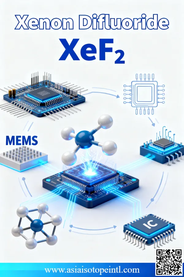
3. XeF₂ in MEMS Device Release: The Flagship Application
3.1 The sacrificial layer problem
Most MEMS devices – accelerometers, gyroscopes, microphones, RF switches, bolometers, micro‑mirrors – are built as multilayer stacks on a silicon wafer. A typical flow uses:
- A sacrificial layer (often poly‑Si or bulk Si) that will later be removed
- A structural layer (poly‑Si, Si₃N₄, metal, parylene, etc.) that forms beams, membranes, or masses
To make the device movable, the sacrificial silicon must be etched away underneath the structural layer. Historically this was done with wet etchants such as KOH or TMAH, but those introduce stiction – the tendency of released structures to stick to the substrate as the liquid dries. Stiction can destroy a large fraction of delicate devices at wafer scale.
3.2 How XeF₂ solved MEMS release
XeF₂’s adoption in MEMS during the mid‑1990s was a major turning point. Because XeF₂ is used in the vapor phase:
- There is no liquid meniscus and therefore no capillary‑force‑induced stiction.
- The process is gentle and residue‑free, producing clean structures ready for anti‑stiction coatings or packaging. https://en.wikipedia.org/wiki/Vapor_etching
Its high selectivity allows the sacrificial silicon (single‑crystal, poly, or amorphous) to be removed while leaving:
- Oxide/nitride support layers
- Metal electrodes and interconnects
- Photoresist or polymer passivation
essentially untouched.
Commercial XeF₂ tools from suppliers such as KLA (Xactix®), memsstar (XERIC™), and Samco are now standard equipment in MEMS fabs specifically for sacrificial vapor release etching.
3.3 Undercut and through‑via release
Because the etch is isotropic, XeF₂ is exceptionally effective at undercutting large distances from a small access window. For example:
- Process notes from university and national labs report undercuts exceeding 100 µm through small release holes without measurable damage to oxide masks.
- Industrial systems promote “large undercuts at high etch rates with no degradation in etch rate” for MEMS release.
A common strategy is to pattern release vias in the top structural layer, expose the underlying sacrificial silicon, and then let XeF₂ laterally etch away the silicon to free beams or membranes. This is precisely how suspended RF membranes, micro‑mirrors, and inertial sensor proof masses are manufactured at scale.
3.4 Typical MEMS use‑cases
In practice, XeF₂ is now entrenched in a broad range of MEMS flows, for example:
- Inertial sensors (accelerometers/gyros) – releasing deep, high‑mass structures under thin caps without stiction or thermal damage.
- RF MEMS switches and tunable capacitors – undercutting silicon beneath metal bridges and membranes while preserving low‑loss metal and dielectric stacks.
- Uncooled IR bolometer arrays – freeing suspended absorber membranes above read‑out electronics without flooding the circuitry with liquids.
- CMOS‑integrated MEMS – using XeF₂ through passivation openings on pre‑processed CMOS wafers, preserving backend metallization and dielectric stacks. https://memsnet.org/about/fabrication.html
Many of these devices simply could not meet reliability and yield targets using wet‑etch release.
4. Beyond the Basics: Advanced MEMS and Microdevice Applications
As process engineers became comfortable with XeF₂, its use expanded far beyond “simple” beam release into more sophisticated architectures.
4.1 Movable SOI structures and high‑aspect‑ratio devices
On silicon‑on‑insulator (SOI) wafers, deep reactive ion etching (DRIE) is often used to define high‑aspect‑ratio structures in the device layer. XeF₂ is then applied to undercut these structures by etching the underlying silicon handle through access openings, effectively freeing single‑crystal silicon resonators, comb drives, and other elements while preserving the buried oxide (BOX). https://www.osti.gov/biblio/1026980
The combination of DRIE + XeF₂ thus allows:
- Very tall, stiff mechanical structures
- Clean, BOX‑defined anchors
- Large undercuts beneath complex geometries
—a powerful recipe for precision timing resonators, high‑Q mechanical filters, and robust inertial sensors.
4.2 Photonic devices, microLEDs, and RF membranes
Tool vendors now explicitly position XeF₂ for photonic and RF applications as well as MEMS:
- KLA’s Xactix® product line lists vapor‑phase XeF₂ as a release etch for MEMS, microLEDs, and RF membranes, leveraging its ability to undercut silicon without disturbing optically critical dielectrics and metals.
- For silicon photonics, XeF₂ can be used to:
- Hollow out buried air gaps around waveguides for index engineering
- Release movable couplers and phase shifters
- Sculpt 3D optical cavities beneath pre‑patterned structures without disturbing their surfaces
In microLED backplanes and RF front‑end modules, XeF₂ enables thin, suspended membranes for thermal or RF isolation while protecting sensitive metallization and passivation layers.
4.3 Microfluidics and buried channel formation
Beyond “classical” MEMS, several groups have demonstrated using XeF₂ to fabricate buried microfluidic channels and hollow structures in silicon:
- At CEITEC and related labs, XeF₂ is used together with DRIE and parylene coatings to create buried microfluidic channels with observation windows, as well as hollow parylene micropillars for mechanosensing. https://www.ceitec.eu/xef2-etching-of-silicon/e1454
The flow is typically:
- Pattern trenches or cavities in silicon
- Seal them with a conformal layer (e.g., parylene, oxide)
- Use XeF₂ to laterally hollow out remaining silicon beneath the cap, leaving an enclosed channel or cavity
Because XeF₂ does not attack polymers like parylene or PDMS, it is particularly well‑suited to these hybrid microfluidic‑MEMS structures. https://www.coral.washington.edu/tools/
4.4 Post‑dicing and in‑package release
A subtle but powerful advantage of XeF₂ is that it can be used after dicing or even after packaging:
- XeF₂ doesn’t attack common dicing adhesives or many packaging materials, and it remains highly selective to silicon in the presence of metals and organics.
- This allows some manufacturers to delay the final MEMS release until after the die is bonded into a package, improving yield by eliminating release‑induced damage on otherwise good die.
Such late‑stage release would be impractical with wet etches and very risky with plasma‑based approaches.
5. XeF₂ in IC Failure Analysis and Circuit Debug
If MEMS release is where XeF₂ first became a “star,” IC failure analysis (FA) and debug is where it shows its finesse as a surgical tool.
5.1 Backside thinning and delayering
A classic challenge in IC FA is gaining optical or spectroscopic access to a buried interface or device layer without destroying it. A NASA tech brief from the mid‑1980s described using XeF₂ to remove large amounts of silicon from integrated‑circuit and solar‑cell structures while leaving SiO₂, Si₃N₄, and Al₂O₃ intact. https://ntrs.nasa.gov/citations/19860000221
In that work, the wafer was etched from the backside:
- Starting from a standard ~300 µm‑thick silicon wafer with a thin oxide layer on the front side, XeF₂ was used to thin the silicon from the back down to a residual Si layer of just a few tens of nanometers.
- The front‑side oxide and metal layers were left undamaged, enabling high‑sensitivity spectroscopic analysis (e.g., of the SiO₂/Al interface).
This same concept underlies many modern FA flows:
- Backside preparation for laser‑based probing (e.g., photon emission microscopy, laser‑voltage probing)
- Backside IR or X‑ray imaging, where minimal silicon thickness is desired for transparency
XeF₂’s selectivity lets FA engineers thin silicon aggressively while preserving delicate front‑end dielectrics and interconnects.
5.2 Local window opening and via formation
Failure analysis and debug often require access to a very specific node, transistor, or wire deep inside the stack. XeF₂ is used to:
- Open local backside or frontside “windows” through silicon to a target layer
- Create micro‑vias for electrical probing or signal injection
Because XeF₂ is isotropic, it can laterally hollow out silicon underneath a small opening, allowing larger probe pads or cavities without increasing mask size. At the same time, surrounding dielectrics and metals remain essentially intact thanks to the high selectivity. https://ntrs.nasa.gov/citations/19860000221
5.3 Gas‑assisted FIB etching and circuit editing
Modern focused ion beam (FIB) systems routinely use gas‑assisted etching (GAE): a reactive gas is injected near the beam impact point to enhance material removal. For silicon and silicon‑based dielectrics, XeF₂ is one of the most important gas chemistries.
Key benefits in the FA context:
- Higher etch rate and better selectivity – the combination of ion sputtering and XeF₂ chemical attack dramatically accelerates local silicon removal while minimizing damage to neighboring layers.
- Reduced redeposition and contamination – XeF₂ turns sputtered silicon into volatile SiF₄, which pumps away instead of re‑depositing on nearby features.
- Sharper, cleaner cross‑sections – essential for accurate SEM inspection of multilayer stacks.
Patents on IC device editing describe FIB systems equipped with gas injection units precisely for this kind of chemically enhanced ion beam etching of interlayer dielectrics and silicon in ICs, enabling rapid exposure and rewiring of internal nodes.
5.4 Emerging: XeF₂ in electron‑beam‑based editing and superconducting / III‑V devices
Beyond gallium‑ion FIB, XeF₂ is now being explored in focused electron‑beam induced etching (FEBIE) and in advanced materials systems:
- Recent work has shown XeF₂‑assisted FEBIE of niobium thin films as a route to on‑the‑fly editing of superconducting devices, achieving etched features down to ~17 nm with relatively low damage.
- Another study demonstrated XeF₂‑enhanced FIB etching of GaSb, where XeF₂ not only improves etch control but also suppresses undesirable nanofibre growth and reduces contamination – highly relevant for III‑V optoelectronic device modification.
These developments point toward a future where XeF₂ is not just a silicon tool, but a general‑purpose micro‑ and nano‑machining assist gas for exotic materials in quantum and photonic ICs.

XeF2 Xenon Difluoride
6. Process Integration, Equipment, and Practical Considerations
6.1 Commercial XeF₂ platforms
What used to be home‑built glassware and manual valves has matured into a robust equipment ecosystem. Today, you’ll find XeF₂ etchers in both university cleanrooms and 200/300 mm production fabs, for example:
- KLA / SPTS Xactix® series (e2, X4, CVE) – single‑wafer tools for R&D through high‑volume MEMS and photonic production; support pulsed and continuous‑flow modes with patented dual‑chamber designs.
- memsstar XERIC™ silicon etch – continuous‑flow XeF₂ modules for advanced dry release and large‑undercut MEMS structures, integrated into ORBIS™ cluster platforms.
- Samco VPE‑4F – compact XeF₂ systems targeted at sacrificial silicon etch for MEMS.
- Numerous home‑built or semi‑custom tools at universities such as USC, Caltech, Vanderbilt, AMOLF and others for selective dry Si etching in R&D environments.
This diversity means engineers can choose between benchtop R&D platforms and fully integrated production modules, depending on volume and cleanliness requirements.
6.2 Integration into MEMS and IC flows
When introducing XeF₂ into a flow, several practical questions arise:
- Mask materials – Oxides and nitrides are typically excellent masks; metals like Al, Au, Ni, Pt and polymers such as photoresist and parylene are also compatible in many recipes.
- Design rules – Layout engineers must size release holes, cavity spans, and sacrificial layer thicknesses to balance undercut distance, etch time, and mechanical stability.
- Loading and uniformity – Process engineers may need to limit exposed Si area per wafer or adjust patterns to maintain uniform etch across the lot.
- Metrology – Transparent chamber lids and in‑situ imaging, pressure‑based endpoint detection, and post‑etch profilometry are all used to control and characterize advanced XeF₂ processes.
Well‑tuned XeF₂ steps often become some of the most repeatable parts of a MEMS flow because they avoid the variability of liquid handling and plasma conditions.
6.3 Throughput and cost
XeF₂ is not a “cheap commodity” gas, and etch chambers are typically single‑wafer or small batch. However:
- The dry, single‑step nature of the process (no pre‑bakes, no wet cleans, no drying sequences) simplifies the overall flow.
- High selectivity reduces the need for very thick masks, saving deposition and patterning time.
- Vapor‑phase etch steps can often be scheduled late in the flow (or post‑dicing), increasing effective die yield.
In many high‑value MEMS and FA applications, the improved yield and reduced re‑work more than compensate for gas and tool costs.
7. Safety, Handling, and Environmental Aspects
XeF₂ deserves respect. While extremely useful, it is also toxic and strongly corrosive in the presence of moisture.
7.1 Hydrolysis and HF formation
In contact with water, XeF₂ decomposes rapidly:
XeF₂ + 2 H₂O → Xe + O₂ + 4 HF
Hydrofluoric acid (HF) is highly corrosive and poses serious health risks. For this reason, XeF₂ must be handled and stored under dry, inert conditions, typically in sealed ampoules or solid hoppers connected to a vacuum manifold.
7.2 Tool‑level safety engineering
Modern tools incorporate:
- Inert gas purges and isolation valves to prevent air/moisture ingress
- Exhaust scrubbers (wet or dry) to neutralize HF, SiF₄, and residual XeF₂
- Interlocks and gas monitoring to shut down the system in case of pressure, flow, or leak anomalies
From an operator standpoint, XeF₂ systems are often no more burdensome than other specialty gas tools once installed, but they require disciplined procedures.
7.3 Recycling and sustainability
There is active work – including patent filings – on recovering and recycling xenon and XeF₂ from process exhaust, for both cost and environmental reasons:
- Cold traps and selective condensation can separate XeF₂, by‑product fluorides (e.g., MoF₆), and inert gases.
- Recovered xenon can be re‑fluorinated with F₂ or via UV‑assisted methods to regenerate XeF₂.
As device volumes and XeF₂ usage grow, these recycling strategies will become increasingly valuable.
8. Outlook: Where Advanced XeF₂ Applications Are Headed
Looking ahead, I see XeF₂ playing an even more strategic role at the intersection of MEMS, advanced logic, photonics, and quantum technologies.
Several trends are clear:
- More complex 3D MEMS and NEMS – as designs move toward multi‑layer, heterogeneous stacks, the need for highly selective, low‑damage sacrificial etches will only increase. XeF₂ is uniquely positioned for these release steps.
- Integration with atomic‑scale processes – combining XeF₂ chemistry with atomic‑layer etching or beam‑based techniques could push silicon (and other materials) structuring into the true nanometer regime, as recent FEBIE and FIB‑GAE work is already suggesting.
- Broader material coverage – evidence that XeF₂ can assist in etching W, Mo, Nb, diamond, and III‑V semiconductors hints at a future where XeF₂ is a go‑to precursor for editing not just CMOS, but superconducting, photonic, and compound‑semiconductor ICs.
- More sustainable gas management – as recycling schemes mature, the cost and environmental footprint of XeF₂ will drop, making its adoption even more attractive across fabs of all sizes.
From MEMS device release to IC failure analysis and nanoscale device editing, Xenon Difluoride has evolved from a niche curiosity into a foundational technology. Its room‑temperature, isotropic, highly selective removal of silicon – and increasingly, other materials – fills a unique and expanding niche that neither wet chemistries nor plasmas can truly replace.
For engineers and scientists designing the next generation of sensors, processors, photonic and quantum devices, a deep understanding of XeF₂ is no longer optional; it is a core part of the advanced manufacturing toolkit.
Would you like a deeper dive into any specific technical parameters or applications?
As an industry leader focused in Specialty Gases products, our goal is to support our customers by keeping them at the forefront of their industries. We’re here to help with any questions you might have so you can transform your ideas into reality, and tackle those big science challenges.
Get free consultant, our experts are ready to serve.
(Follow up our update articles on www.asiaisotopeintl.com or send your comments to tao.hu@asiaisotope.com for further communications)