XeF2 Vapor Phase Etching: Why High-Selectivity Silicon Removal Transforms Semiconductor Manufacturing
BY Tao, Published Jan 3, 2026
Introduction: The Unseen Revolution in Chip Fabrication
Over the past 3 years, China Isotope Development Co Ltd was starting to supply Xenon Difluoride (XeF₂) to China domestic clients, I have observed that true breakthroughs in semiconductor manufacturing are rarely about a single, dramatic invention. Instead, they are often driven by the mastery of highly specialized materials that solve fundamental, persistent challenges. Xenon Difluoride (XeF₂), a seemingly exotic crystalline solid, is one such transformative agent. While it may not have the household recognition of silicon, its impact on the industry is profound and indispensable.
The relentless pursuit of Moore’s Law—the observation that the number of transistors on a microchip doubles approximately every two years—has pushed fabrication techniques to their absolute physical limits. As we build smaller, faster, and more complex three-dimensional structures, the methods used to sculpt silicon become critically important. Traditional etching processes, whether wet chemical baths or aggressive plasma-based methods, often introduce collateral damage, compromise structural integrity, or simply lack the precision required for next-generation devices.
This is where XeF₂ vapor phase etching emerges not merely as an alternative, but as a paradigm-shifting enabler. Its defining characteristic—extraordinarily high selectivity for silicon—allows engineers to perform surgical material removal at the nanoscale, leaving adjacent, delicate materials completely untouched. This article will provide an expert’s perspective on why XeF₂ vapor phase etching is more than just a process; it is a foundational technology that unlocks new possibilities in MEMS, advanced logic, failure analysis, and beyond. We will explore its underlying chemistry, its unparalleled advantages, and the specific applications where it has become the undisputed gold standard.
A Primer on Xenon Difluoride (XeF₂): From Chemical Curiosity to Industrial Workhorse
To appreciate its role, one must first understand the unique nature of Xenon Difluoride itself. XeF₂ was one of the first noble gas compounds ever synthesized, a discovery that shattered the long-held belief that gases like xenon were chemically inert. From a materials science perspective, its properties are a perfect storm for high-precision etching.
Physical and Chemical Profile:
- Appearance and State: At room temperature, XeF₂ is a dense, white, crystalline solid. Its most crucial property for this application is its high vapor pressure, which allows it to sublime—transition directly from a solid to a gas—at a controlled rate even under modest vacuum and near-ambient temperatures. This eliminates the need for complex liquid delivery systems.
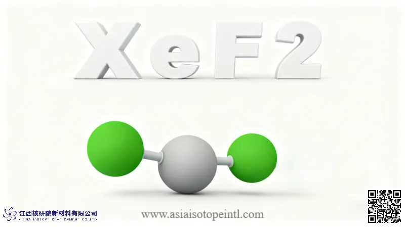
- Molecular Structure: The XeF₂ molecule has a linear geometry (F-Xe-F). The central xenon atom is surrounded by fluorine atoms, which are highly electronegative. This configuration makes XeF₂ a potent fluorinating agent, meaning it is exceptionally effective at donating fluorine atoms to other elements.
- Reactivity: This is where the magic happens. XeF₂ reacts spontaneously and exothermically with silicon (Si). However, it is remarkably unreactive towards many other materials commonly found in semiconductor fabrication, including silicon dioxide (SiO₂), silicon nitride (Si₃N₄), photoresists, and metals like aluminum (Al) and copper (Cu). This inherent chemical preference is the basis for its high selectivity.
In essence, XeF₂ is a “smart” etchant. It doesn’t require the brute force of high-energy plasma or the indiscriminate nature of strong acids. Instead, it leverages fundamental chemical principles to seek out and remove silicon with surgical precision.
The Mechanism: How Spontaneous Vapor Phase Etching Works
The term “vapor phase etching” describes a process where a gaseous reactant removes a solid material by forming a volatile product. The XeF₂ process is a textbook example of this and is elegantly simple, involving no plasma, high temperatures, or external energy sources.
The etching process can be broken down into a few key steps:
- Transport and Adsorption: Solid XeF₂ is placed in a controlled chamber connected to the main process chamber containing the silicon wafer. As the XeF₂ sublimes, its vapor flows into the process chamber and the gaseous molecules adsorb (stick) onto the surface of the wafer.
- Surface Reaction: Once adsorbed on the silicon surface, the XeF₂ molecules dissociate. The highly reactive fluorine atoms attack the silicon lattice, breaking Si-Si bonds.
- Product Formation and Desorption: The reaction between silicon and fluorine forms silicon tetrafluoride (SiF₄), a highly volatile gas. This gaseous product immediately desorbs (detaches) from the surface, exposing fresh silicon for the reaction to continue. The other byproduct is inert xenon (Xe) gas.
The overall chemical reaction is: 2XeF₂ (gas) + Si (solid) → 2Xe (gas) + SiF₄ (gas)
A critical feature of this process is that it is isotropic, meaning it etches uniformly in all directions (downward and sideways). While anisotropic (directional) etching is desired for creating vertical trenches, isotropic etching is essential for undercutting and hollowing out structures, a key requirement in many advanced applications.

The Unmatched Advantage: Defining High-Selectivity in a Real-World Context
The term “high selectivity” is the cornerstone of XeF₂’s value proposition. In semiconductor manufacturing, selectivity is a quantitative measure of how much faster an etchant removes the target material compared to the masking material. It is expressed as a ratio.
- Conventional Plasma Etching (e.g., using SF₆): Might achieve a selectivity of 50:1 for silicon over silicon dioxide. This means for every 50 nanometers of silicon removed, 1 nanometer of the oxide mask is also eroded.
- XeF₂ Vapor Phase Etching: Routinely achieves selectivities of 1000:1 or even higher for silicon over silicon dioxide, silicon nitride, and photoresist.
This thousand-fold improvement is not merely an incremental gain; it is a complete game-changer. It means an engineer can perform a deep silicon etch for an extended period without any meaningful degradation of the critical masking layers or adjacent functional structures. This level of precision prevents device failure, improves performance, and dramatically increases manufacturing yield.
The reason for this incredible selectivity lies in the reaction chemistry. The energy barrier for XeF₂ to react with the strong Si-O bonds in silicon dioxide or the Si-N bonds in silicon nitride is significantly higher than for the Si-Si bonds in pure silicon. At room temperature, the reaction with silicon proceeds readily, while the reactions with the oxide and nitride are kinetically hindered, proceeding at a negligible rate.
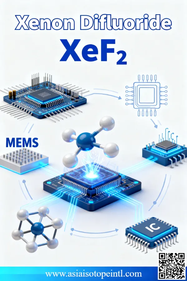
Transforming Semiconductor Manufacturing: Key Applications Unlocked by XeF₂
The theoretical advantages of XeF₂ translate directly into solutions for some of the industry’s most difficult manufacturing challenges.
1. MEMS Fabrication: The Foundation of the Sensor Revolution
Microelectromechanical Systems (MEMS) are miniature machines like accelerometers, gyroscopes, microphones, and micro-mirrors. These devices feature microscopic moving parts (beams, membranes, gears) that must be physically freed from the underlying silicon substrate. This “release” step is where XeF₂ shines.
- The Challenge: A structural layer (e.g., polysilicon or silicon nitride) is built on top of a “sacrificial” silicon layer. This sacrificial layer must be completely removed without damaging the delicate, suspended structure above it. Wet etching methods using liquids cause “stiction,” where surface tension pulls the released structure down, permanently sticking it to the substrate and rendering the device useless.
- The XeF₂ Solution: As a completely dry, vapor-phase process, XeF₂ etching eliminates stiction entirely. Its isotropic nature allows it to perfectly undercut large structures, hollowing out the sacrificial silicon from beneath. Its high selectivity ensures that the functional MEMS structure, often protected by a thin layer of oxide or nitride, remains pristine. Today, virtually every high-performance MEMS device, from the accelerometer in your smartphone to the pressure sensor in a medical device, relies on XeF₂ for this critical release step.
2. IC Failure Analysis and Circuit Edit: The Semiconductor Detective’s Tool
When a multi-billion dollar chip design fails during testing, finding the root cause is a high-stakes race against time. Engineers must perform “nanosurgery” to probe and modify the chip’s internal circuitry.
- The Challenge: To access a specific transistor or metal line deep within a chip, layers of material must be painstakingly removed. Modern chips often use a layer of cobalt or nickel silicide on top of the silicon transistor gate to reduce resistance. Removing this silicide and the underlying silicon to expose the gate structure without damaging the surrounding metal interconnects and insulating dielectrics is exceptionally difficult with conventional methods.
- The XeF₂ Solution: XeF₂ is the perfect tool for this delicate operation. It can selectively etch away the silicon and silicide layers while leaving the metallic and oxide components completely intact. This allows failure analysis engineers to create a “window” into the chip’s core, enabling them to probe electrical signals, identify defects, and even use focused ion beams (FIB) to cut or rewire circuits. This capability can shorten chip debug cycles by weeks or months, saving millions of dollars in development costs.
3. Advanced Transistor Architectures: Enabling the Future of Logic
As transistors shrink below the 5-nanometer node, the traditional FinFET architecture is giving way to Gate-All-Around (GAA) structures, also known as nanosheets or nanowires.
- The Challenge: In a GAAFET, the channel (where current flows) is a stack of ultra-thin silicon nanosheets that are completely surrounded by the gate material. During fabrication, these silicon nanosheets are initially embedded within layers of a sacrificial material, typically silicon-germanium (SiGe). This sacrificial SiGe must be removed with absolute perfection to create the space for the gate material, without damaging the fragile silicon nanosheets.
- The XeF₂ Solution: While other etchants are being explored, XeF₂’s fundamental properties make it a leading candidate for this process. Its ability to selectively remove silicon-based materials (like SiGe, which it etches even faster than pure Si) while preserving others is critical. The gentle, damage-free nature of the vapor phase process is essential for maintaining the integrity of the sub-3-nanometer thick nanosheets. As leading foundries like Samsung and Intel adopt GAA technology, the role of highly selective dry etching becomes more crucial than ever.
A Comparative Analysis: XeF₂ vs. Alternative Etching Technologies
To fully appreciate its transformative power, it’s useful to place XeF₂ in context with its alternatives.
| Feature | XeF₂ Vapor Etching | Wet Chemical Etching (e.g., KOH, HF) | Plasma Etching (e.g., RIE, DRIE) |
|---|---|---|---|
| Selectivity (Si vs. SiO₂) | Extremely High (>1000:1) | Moderate (100:1 for KOH) to Low (HF attacks oxide) | Low to Moderate (10:1 to 100:1) |
| Process Type | Dry Vapor Phase | Wet Liquid Phase | Dry Plasma Phase |
| Stiction Risk | None | Very High | Low, but can occur from byproducts |
| Device Damage | Minimal to None (no ions, no high temp) | Can cause contamination and material attack | High risk of plasma-induced damage (PID) |
| Isotropy | Highly Isotropic | Isotropic or crystallographic | Primarily Anisotropic (directional) |
| Operating Temperature | Room Temperature | Elevated (50-80°C) | Room Temperature to Cryogenic |
| Complexity & Cost | Moderate equipment cost, simple process | Low equipment cost, complex handling/disposal | High equipment cost, complex process control |
This comparison makes it clear: for applications requiring isotropic, damage-free, and ultra-high-selectivity silicon removal, XeF₂ operates in a class of its own.
Conclusion: An Indispensable Tool for the Nanoscale Era
Xenon Difluoride vapor phase etching is far more than a niche laboratory technique; it is a cornerstone of modern, high-volume semiconductor manufacturing. Its unique ability to remove silicon with near-perfect selectivity and without the collateral damage associated with wet or plasma processes has been instrumental in enabling the entire MEMS industry. Furthermore, its precision has made it an invaluable tool for debugging the world’s most complex microchips and a critical enabler for the next generation of transistor architectures.
From my perspective as a materials expert, the story of XeF₂ is a powerful testament to how a deep understanding of chemistry can solve intractable engineering problems. It is a chemical scalpel that allows us to sculpt silicon at the atomic level, transforming what is possible in the world of microfabrication. As we continue to push the boundaries of what can be built on a chip, the demand for such precise and elegant manufacturing solutions will only grow, cementing Xenon Difluoride’s legacy as a quiet but powerful force shaping our technological future.
Would you like a deeper dive into any specific technical parameters or applications?
As an industry leader focused in Specialty Gases products, our goal is to support our customers by keeping them at the forefront of their industries. We’re here to help with any questions you might have so you can transform your ideas into reality, and tackle those big science challenges.
Get free consultant, our experts are ready to serve.
(Follow up our update articles on www.asiaisotopeintl.com or send your comments to tao.hu@asiaisotope.com for further communications)