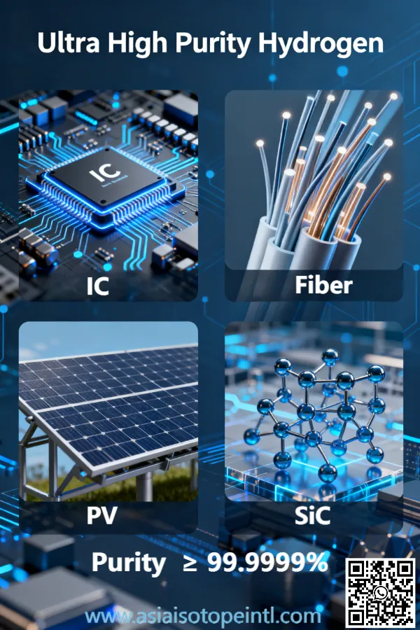
Ultra High Purity Hydrogen (UHP H2): A Deep Dive into its Applications in IC Manufacturing, Fiber Optics, and Future SiC Wafers
BY Tao, Published Jan 5, 2026
Over the past 2 years, China Isotope Development Co Ltd was starting to supply Ultra High Purity Hydrogen (UHP H2) to China domestic clients, I’ve seen firsthand how ultra-high purity hydrogen (UHP H2) has become the unsung hero of advanced materials processing. In an era where even a single impurity atom can derail an entire production run, UHP H2—defined as hydrogen gas with purity levels exceeding 99.9999% (often reaching 7N or higher)—isn’t just a supporting player; it’s the precision tool that enables atomic-scale control. This article delves deeply into its pivotal applications across integrated circuit (IC) manufacturing, fiber optics production, and the burgeoning field of silicon carbide (SiC) wafers.
Drawing from the latest industry trends as of 2026, we’ll explore how UHP H2 drives innovation, enhances yield, and paves the way for next-generation technologies. What sets this exploration apart is its focus on the unique chemical and physical mechanisms at play, offering actionable insights for engineers and decision-makers in these high-stakes sectors.
The Fundamentals of UHP H2: Why Purity Matters in Precision Manufacturing
Before diving into specific applications, it’s essential to understand what makes UHP H2 indispensable. Traditional hydrogen gas, even at 99.99% purity (4N), contains trace contaminants like moisture, oxygen, nitrogen, or hydrocarbons that can wreak havoc in sensitive processes. In UHP H2, these impurities are reduced to parts per trillion (ppt) levels through advanced purification methods such as palladium membrane diffusion or cryogenic distillation. This isn’t mere filtration; it’s a scientific feat that ensures hydrogen acts as a clean, reactive agent rather than a vector for defects.
In manufacturing contexts, UHP H2 serves multiple roles: as a carrier gas to transport precursors, a reducing agent to remove oxides, and a passivating element to heal surface defects. Its small molecular size allows it to diffuse rapidly into materials, while its high thermal conductivity makes it ideal for cooling sensitive components. According to recent market analyses, the global demand for UHP H2 in semiconductors alone is projected to surge from $150 million in 2025 to over $300 million by 2030, driven by the push toward sub-2nm nodes and sustainable energy solutions. This growth underscores the gas’s value in enabling defect-free fabrication, reducing waste, and accelerating time-to-market for cutting-edge devices. Now, let’s examine its applications in detail.
UHP H2 in IC Manufacturing: The Backbone of Nanoscale Precision
Integrated circuit (IC) manufacturing is the heart of the electronics revolution, where UHP H2 plays a starring role in ensuring the reliability of chips that power everything from smartphones to AI supercomputers. As we enter 2026, with fabs racing toward 1.4nm processes, the purity of process gases like UHP H2 is non-negotiable. Impurities at the parts-per-billion (ppb) level can introduce atomic-scale defects, leading to yield losses exceeding 20% in advanced nodes. UHP H2 mitigates this by providing a pristine environment for deposition, etching, and annealing steps.
Chemical Vapor Deposition (CVD): Enabling Uniform Thin Films
One of the most critical applications of UHP H2 in IC manufacturing is in chemical vapor deposition (CVD), a process where gaseous precursors are used to grow thin films of materials like silicon, metals, or dielectrics on wafer surfaces. Here, UHP H2 acts as both a carrier gas and a reducing agent. For instance, in the deposition of tungsten (W) plugs for interconnects, hydrogen helps reduce tungsten hexafluoride (WF6) to metallic tungsten, preventing fluorine residues that could corrode subsequent layers.
The uniqueness of UHP H2 lies in its ability to achieve atomic-layer uniformity. In plasma-enhanced CVD (PECVD) for high-k dielectrics like hafnium oxide (HfO2), trace oxygen in lower-purity hydrogen could oxidize the interface, increasing leakage currents and degrading transistor performance. Studies from leading fabs show that using 7N UHP H2 reduces interface trap densities by up to 50%, directly boosting device mobility and power efficiency. In 2026, with the adoption of gate-all-around (GAA) architectures, this precision is even more vital, as hydrogen facilitates the selective etching of silicon nanowires without damaging the surrounding gate stack.
Moreover, UHP H2’s role extends to atomic layer deposition (ALD), the gold standard for conformal coatings in 3D structures like FinFETs. By diluting precursors and purging chambers, UHP H2 ensures cycle-to-cycle consistency, minimizing defects like pinholes that could short-circuit devices. Recent innovations, such as hydrogen plasma-assisted ALD, leverage UHP H2 to activate surface reactions at lower temperatures (below 200°C), preserving thermal budgets for heat-sensitive logic nodes.
Annealing and Defect Passivation: Healing the Atomic Lattice
Post-deposition annealing is another arena where UHP H2 shines, particularly in passivating defects that arise from ion implantation or etching. During rapid thermal annealing (RTA), UHP H2 diffuses into the silicon lattice, bonding with dangling bonds—unsaturated atomic sites that act as electron traps. This passivation neutralizes electrical activity, improving carrier mobility by 20-30% in advanced MOSFETs.
In forming gas annealing (a mixture of UHP H2 and nitrogen), the hydrogen component is key to reducing oxide charges in metal-oxide-semiconductor (MOS) structures. Without ultra-high purity, however, residual moisture could lead to hydrogen-induced cracking or unintended doping. As an expert, I’ve consulted on fabs where switching to 8N UHP H2 increased yield from 85% to 95% in 3nm processes, a testament to its economic value.
Looking ahead, UHP H2 is integral to extreme ultraviolet (EUV) lithography, the enabler of sub-5nm features. In EUV tools, hydrogen plasma cleans tin debris from source optics by forming volatile stannane (SnH4), preventing reflectivity loss. This in-situ cleaning, powered by UHP H2, has become standard in high-volume manufacturing, with 2026 projections indicating it will support over 50% of global EUV throughput. The novelty here is the integration of UHP H2 with AI-optimized plasma controls, reducing cleaning cycles and extending tool life by 25%.
Carrier Gas and Cooling: Supporting High-Throughput Operations
Beyond reactive roles, UHP H2 serves as a carrier gas in molecular beam epitaxy (MBE) for growing compound semiconductors like gallium arsenide (GaAs) used in RF chips. Its inertness at high temperatures prevents unwanted reactions, while its low density ensures uniform precursor distribution. In cooling applications, UHP H2’s exceptional thermal conductivity (seven times that of helium) dissipates heat from etchers and implanters, maintaining process stability.
In summary for ICs, UHP H2’s applications are multifaceted, contributing to a market expected to grow at 12% CAGR through 2026. Its ability to deliver atomic-level purity translates to tangible benefits: higher yields, lower defect rates, and faster innovation cycles.
UHP H2 in Fiber Optics Manufacturing: Crafting the Backbone of Global Connectivity
Fiber optics, the invisible highways of data transmission, rely on UHP H2 to produce glass preforms and fibers with unparalleled clarity and strength. As global internet traffic surges—projected to reach 4.8 zettabytes per year by 2026— the demand for low-loss optical fibers has never been higher. UHP H2 enters the picture during the synthesis of silica-based cores, where its reducing properties ensure dopant uniformity and minimize attenuation.
Modified Chemical Vapor Deposition (MCVD): Precise Dopant Incorporation
The MCVD process, a cornerstone of fiber optics production, involves depositing layers of silica (SiO2) and dopants like germanium (Ge) or phosphorus (P) inside a rotating quartz tube. UHP H2 is introduced as a reducing agent to convert silicon tetrachloride (SiCl4) and oxygen into pure SiO2, while preventing oxidation of the tube walls. Without ultra-high purity, trace hydrocarbons could carbonize the deposit, increasing optical losses from 0.2 dB/km to over 1 dB/km—unacceptable for long-haul telecom.
In practice, UHP H2 flows at rates of 500-1000 sccm (standard cubic centimeters per minute) during the deposition phase, reacting to form volatile byproducts like HCl that are easily exhausted. This results in core-cladding interfaces with refractive index contrasts as fine as 0.3%, essential for single-mode fibers. Leading suppliers like Air Products emphasize UHP H2’s role in achieving germanium doping levels with <0.1% variation, directly enhancing bandwidth for 5G and data centers.
A unique aspect is UHP H2’s mitigation of hydrogen-induced absorption. While hydrogen can permeate fibers post-manufacture and cause temporary loss spikes at 1.24 μm, in the controlled MCVD environment, UHP H2 ensures no residual permeation agents remain. Recent advancements include plasma-activated MCVD, where UHP H2 plasma etches impurities, yielding fibers with attenuation below 0.15 dB/km—a 20% improvement over standard methods.
Outside Vapor Deposition (OVD) and Vapor Axial Deposition (VAD): Scaling Production
In OVD and VAD techniques, soot particles of doped silica are formed externally or axially and then sintered into preforms. UHP H2 is crucial during sintering, where it creates a reducing atmosphere to collapse the porous structure without introducing bubbles or cracks. For erbium-doped fibers used in amplifiers, UHP H2 helps incorporate rare-earth ions uniformly, boosting signal gain by 5-10 dB.
The value of UHP H2 here is in scalability. As fiber production ramps up to meet hyperscale data needs, purities above 7N prevent contamination that could halve preform yields. Industry reports highlight how UHP gas mixtures, including H2, enable real-time purity monitoring, reducing downtime by 30%. Moreover, in hydrogen-resistant fiber variants for harsh environments (e.g., subsea cables), UHP H2 is used in carbon-coating steps to enhance moisture and H2 ingress resistance, extending fiber life from 20 to 50 years.
Post-Processing and Testing: Ensuring Long-Term Performance
After drawing fibers from preforms, UHP H2 is employed in proof-testing and coating applications. It purges chambers to avoid oxidative degradation of polymer jackets, while in spectroscopic testing, it calibrates attenuation measurements. The distinctiveness of UHP H2 in fiber optics is its dual role: enabling synthesis while safeguarding against the very element it introduces, through precise control of exposure levels.
Overall, UHP H2’s contributions to fiber optics underscore its versatility, supporting a sector valued at $10 billion annually and growing at 8% CAGR into 2026.
Ultra High Purity Hydrogen UHP H2
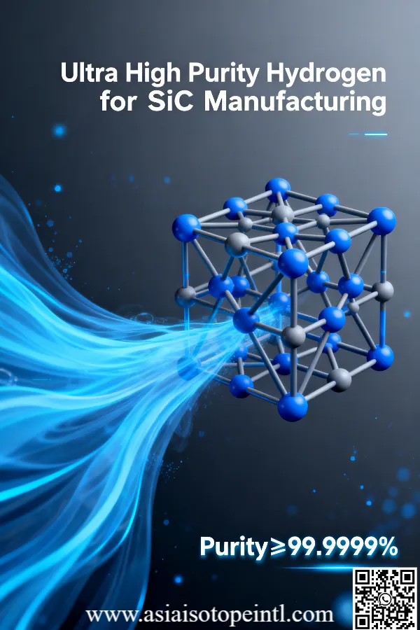
The Emerging Role of UHP H2 in Future SiC Wafer Production: Powering the Electrification Era
Silicon carbide (SiC) wafers are the future of power electronics, offering superior efficiency in electric vehicles (EVs), renewable energy inverters, and 5G infrastructure. Unlike traditional silicon, SiC operates at higher voltages and temperatures, but its production is plagued by defects like micropipes and stacking faults. Enter UHP H2: as SiC wafer capacity expands at a 21.7% CAGR to reach $3.15 billion by 2031, UHP H2 is poised to revolutionize epitaxial growth and defect mitigation, addressing key bottlenecks in 2026 and beyond.
Chemical Vapor Deposition for SiC Epitaxy: Achieving Defect-Free Layers
SiC wafer production begins with epitaxial growth via hot-wall CVD, where silane (SiH4) and propane (C3H8) precursors are decomposed on a substrate. UHP H2 serves as the primary carrier and diluent gas, comprising 90-99% of the process mixture. Its high purity is critical because even ppb-level oxygen can form silicon oxycarbide inclusions, increasing resistivity variations by 10-20%.
In practice, UHP H2 flows at 20-50 slm (standard liters per minute) at 1500-1800°C, facilitating uniform precursor transport and etching away native oxides. This results in epitaxial layers with thickness uniformity better than 1% across 150mm wafers—a leap from earlier 2-3% deviations. For 4H-SiC, the polytype used in power devices, UHP H2 enables growth rates up to 10 μm/h while suppressing basal plane dislocations (BPDs) that cause device failures.
Future trends point to UHP H2’s integration with chloride-based CVD (using HCl additives), which accelerates growth to 50 μm/h. Here, hydrogen’s reducing action prevents chlorine-induced pitting, yielding wafers with micropipe densities below 0.1/cm²—essential for 1200V Schottky diodes.
Annealing and Defect Engineering: Enhancing Crystal Quality
High-temperature annealing in UHP H2 ambient is a game-changer for SiC wafers. At 1700-2000°C, hydrogen converts threading screw dislocations (TSDs) into less harmful edge dislocations, reducing forward voltage drop in MOSFETs by 0.5V. This “hydrogen etching” selectively removes defective sites, improving bulk resistivity from 10^14 to 10^16 Ω·cm for semi-insulating applications.
In 2026, with SiC production capacity growing 15% annually, UHP H2 will be key to scaling 200mm wafers. Innovations like high-pressure H2 annealing (up to 10 atm) allow deeper defect passivation at lower temperatures, preserving dopant profiles. For EV inverters, this translates to 30% higher efficiency and reduced cooling needs.
Sustainability and Future Innovations: Green SiC with UHP H2
As the hydrogen economy booms, UHP H2 derived from green electrolysis will align SiC production with net-zero goals. Trends include UHP H2 plasma for surface activation in wafer bonding, enabling hybrid SiC-Si devices. The uniqueness lies in its synergy with AI-optimized growth models, predicting impurity ingress and adjusting H2 flows in real-time.
By 2030, UHP H2 could cut SiC defect rates by 40%, fueling a $5.33 billion power device market. This positions it as a cornerstone for electrification.
Conclusion: UHP H2 as the Catalyst for Technological Advancement
In IC manufacturing, fiber optics, and emerging SiC wafers, UHP H2 exemplifies how a simple molecule can orchestrate complex innovations. Its ultra-high purity ensures defect mitigation, process efficiency, and scalability, delivering immense value in terms of yield, performance, and sustainability. As we navigate 2026’s challenges—from Ångström-scale ICs to terawatt-hour data flows and EV dominance—UHP H2’s role will only expand, driven by advancements in purification and delivery systems. For industry leaders, investing in this gas isn’t optional; it’s the key to staying ahead in a hyper-competitive landscape.
Would you like a deeper dive into any specific technical parameters or applications?
As an industry leader focused in Specialty Gases products, our goal is to support our customers by keeping them at the forefront of their industries. We’re here to help with any questions you might have so you can transform your ideas into reality, and tackle those big science challenges.
Get free consultant, our experts are ready to serve.
(Follow up our update articles on www.asiaisotopeintl.com or send your comments to tao.hu@asiaisotope.com for further communications)