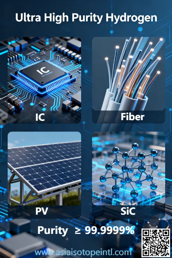
Beyond 99.999%: Why 6N Ultra High Purity Hydrogen is the Gold Standard for IC Fabrication and Epitaxial Growth
BY Tao, Published Jan 5, 2026
Introduction: The Invisible Foundation of the Digital Age
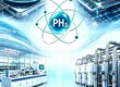
In the pristine cleanrooms where computer chips are born, an invisible yet critical component flows through sophisticated delivery systems—ultra-high purity hydrogen gas. While the general public marvels at the latest smartphone or artificial intelligence breakthrough, few realize that these technological wonders depend fundamentally on gases so pure that their impurity levels are measured in parts per billion. Among these essential materials, 6N hydrogen (99.9999% purity) has emerged as the undisputed gold standard for integrated circuit (IC) fabrication and epitaxial growth processes.
Over the past 2 years, China Isotope Development Co Ltd was starting to supply Ultra High Purity Hydrogen (UHP H2) to China domestic clients in semiconductor manufacturing, I can attest that the journey from industrial-grade hydrogen to 6N purity represents one of the most remarkable achievements in materials science. This article explores why this extraordinary level of purity isn’t just a luxury—it’s an absolute necessity for producing the advanced semiconductors that power our modern world.
Understanding Purity Grades: What Does 6N Really Mean?
The Mathematics of Purity
When we talk about 6N hydrogen, we’re referring to a purity level of 99.9999%—six nines after the decimal point. This means that in every million molecules of gas, only one molecule is an impurity. To put this in perspective, if we had a swimming pool filled with 6N hydrogen, the total volume of impurities would be less than a single drop of water.
The semiconductor industry uses a standardized nomenclature for gas purity:
- 3N (99.9%) – Three nines
- 4N (99.99%) – Four nines
- 5N (99.999%) – Five nines
- 6N (99.9999%) – Six nines
- 7N (99.99999%) – Seven nines
The Quantum Leap from 5N to 6N
The difference between 5N and 6N might seem trivial—just one additional nine. However, this represents a ten-fold reduction in impurity levels, from 10 parts per million (ppm) to 1 ppm. Achieving this leap requires exponentially more sophisticated purification technologies and quality control measures. Each additional nine typically increases production costs by a factor of three to five, reflecting the enormous technical challenges involved.
The Critical Role of Hydrogen in Semiconductor Manufacturing
Epitaxial Growth: Building Crystal Perfection
Epitaxial growth is the process of depositing crystalline layers on a substrate with atomic-level precision. In this process, hydrogen serves multiple crucial functions:
Carrier Gas Function: Hydrogen acts as the primary carrier gas in metal-organic chemical vapor deposition (MOCVD) and vapor phase epitaxy (VPE) systems. Its low molecular weight and high thermal conductivity ensure uniform temperature distribution and efficient transport of precursor materials to the substrate surface.
Reducing Atmosphere: During epitaxial growth, hydrogen creates a reducing environment that prevents oxidation of the growing crystal surface. Even trace amounts of oxygen can create defects that propagate through the entire crystal structure, rendering the device useless.
Surface Cleaning: Before deposition begins, hydrogen helps remove native oxides and organic contaminants from the substrate surface through a process called hydrogen bake. At temperatures above 800°C, hydrogen reduces surface oxides to water vapor, which is then swept away, leaving behind an atomically clean surface ready for epitaxial growth.
IC Fabrication: Precision at the Atomic Scale
In integrated circuit fabrication, hydrogen plays equally vital roles:
Annealing Processes: After ion implantation, semiconductor wafers undergo hydrogen annealing to repair crystal damage and activate dopants. The hydrogen atoms penetrate the crystal lattice, passivating dangling bonds and reducing interface states that would otherwise degrade device performance.
Chemical Vapor Deposition: In processes like plasma-enhanced CVD (PECVD) for depositing silicon nitride or silicon oxide films, hydrogen serves as both a reactant and a carrier gas. The purity of hydrogen directly affects film quality, uniformity, and electrical properties.
Plasma Etching: Hydrogen-based plasmas are used for selective etching of materials like photoresist and organic films. Impurities in the hydrogen can alter plasma chemistry, leading to non-uniform etching rates and compromised device geometries.
Why Impurities Matter: The Domino Effect of Contamination
Types of Critical Impurities
In 6N hydrogen, we monitor several categories of impurities, each with unique impacts on semiconductor processes:
Moisture (H₂O): Even at sub-ppm levels, water vapor can cause oxidation of sensitive materials, alter growth rates in epitaxial processes, and create hydroxyl groups that act as trap states in electronic devices. In advanced node technologies (7nm and below), moisture levels must be controlled below 100 parts per billion (ppb).
Oxygen (O₂): Oxygen contamination leads to unwanted oxide formation, creating interface states that increase leakage currents and reduce carrier mobility. In gallium arsenide (GaAs) epitaxy, oxygen incorporation creates deep-level traps that significantly degrade optical and electrical properties.
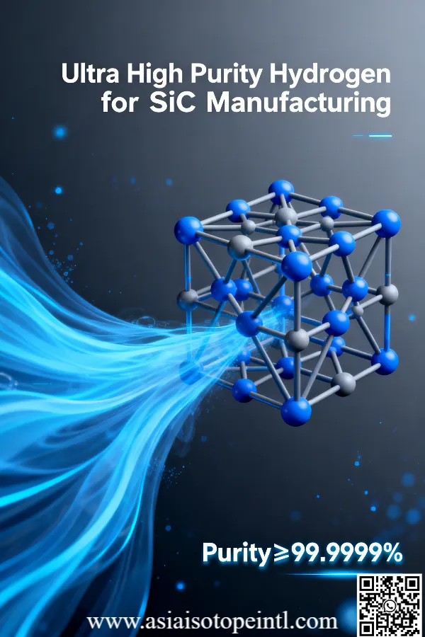
Hydrocarbons (CₙHₘ): Organic contaminants can decompose during high-temperature processes, leaving carbon residues that act as unintentional dopants. In silicon carbide (SiC) epitaxy, hydrocarbon contamination can alter the carbon-to-silicon ratio, affecting material properties fundamentally.
Nitrogen (N₂): While often considered inert, nitrogen can incorporate into certain semiconductor materials as an unintentional dopant. In gallium nitride (GaN) growth, excess nitrogen from gas-phase impurities can create anti-site defects and alter electrical compensation.
Metal Particles: Trace metal contamination, even at parts per trillion levels, can create killer defects in semiconductor devices. Metals like iron, copper, and sodium are particularly problematic as they have high diffusion coefficients in silicon and can migrate through the device structure during processing.
The Multiplication Effect
In semiconductor manufacturing, contamination effects multiply through the production process. A single impurity atom incorporated during epitaxial growth can:
- Create a crystal defect that propagates through subsequent layers
- Alter local electrical fields, affecting nearby device regions
- Serve as a nucleation site for further defect formation
- Increase susceptibility to electromigration and other reliability issues
This multiplication effect means that what starts as a one-in-a-million impurity can ultimately affect device yield by several percentage points—potentially costing millions of dollars in lost revenue for a semiconductor fab.
The Technology Behind 6N Purification
Pressure Swing Adsorption (PSA)
The journey to 6N purity typically begins with pressure swing adsorption, a process that exploits the differential adsorption of gases on molecular sieves. In a typical PSA system:
- Compressed feed gas enters a vessel packed with specialized adsorbent materials
- Impurities like nitrogen, oxygen, and hydrocarbons preferentially adsorb onto the surface
- Pure hydrogen passes through while impurities remain trapped
- The vessel is depressurized to regenerate the adsorbent, releasing trapped impurities
Modern PSA systems use multiple vessels in parallel, allowing continuous operation while maintaining consistent purity levels.
Palladium Membrane Diffusion
For achieving 6N purity, palladium membrane diffusion provides the ultimate purification step. This technology leverages hydrogen’s unique ability to dissociate on palladium surfaces and diffuse through the metal lattice as atomic hydrogen:
- Molecular hydrogen (H₂) adsorbs on the palladium surface
- H₂ dissociates into atomic hydrogen (H)
- Atomic hydrogen diffuses through the palladium lattice
- Hydrogen atoms recombine on the opposite surface, emerging as ultra-pure H₂
Since only hydrogen can traverse the palladium membrane through this mechanism, virtually all impurities are rejected, achieving purities beyond 99.99999% when properly implemented.
Catalytic Purification
Catalytic converters remove specific impurities through chemical reactions:
- Deoxo Catalysts: Convert oxygen to water through reaction with hydrogen
- Hydrogenation Catalysts: Convert unsaturated hydrocarbons to saturated forms that are easier to remove
- Methanation Catalysts: Convert carbon monoxide and carbon dioxide to methane and water
These catalytic stages are carefully sequenced and operated under optimized conditions to maximize impurity removal while minimizing catalyst degradation.
Cryogenic Distillation
For removing impurities with similar chemical properties to hydrogen, cryogenic distillation exploits differences in boiling points. At temperatures near 20 Kelvin (-253°C), hydrogen liquefies while impurities with different volatilities can be separated through fractional distillation. This energy-intensive process is typically reserved for special applications requiring ultra-high purity or isotopic separation.
Quality Assurance: Measuring the Immeasurable
Advanced Analytical Techniques
Verifying 6N purity requires analytical instruments capable of detecting impurities at sub-ppm levels:
Atmospheric Pressure Ionization Mass Spectrometry (APIMS): This technique can detect impurities down to parts per trillion levels. By ionizing gas molecules at atmospheric pressure and analyzing their mass-to-charge ratios, APIMS provides real-time monitoring of multiple impurity species simultaneously.
Cavity Ring-Down Spectroscopy (CRDS): Using laser absorption techniques, CRDS measures moisture levels below 10 ppb with exceptional accuracy. The technique measures the decay rate of light in an optical cavity, providing sensitivity orders of magnitude better than traditional absorption spectroscopy.
Gas Chromatography with Multiple Detectors: Modern GC systems employ various detectors optimized for different impurities:
- Thermal conductivity detectors for permanent gases
- Flame ionization detectors for hydrocarbons
- Electron capture detectors for electronegative species
- Mass spectrometry for comprehensive analysis
Continuous Monitoring Systems
Modern semiconductor fabs implement continuous monitoring systems that track hydrogen purity in real-time:
- Point-of-Use Monitors: Installed at tool interfaces to verify purity at the critical point of consumption
- Distribution System Monitors: Track purity throughout the gas delivery network
- Alarm Systems: Trigger immediate notifications if purity drops below specifications
- Data Logging: Create comprehensive records for process control and troubleshooting
Economic Considerations: The Cost-Benefit Analysis
The Price of Purity
Producing 6N hydrogen costs approximately 10-15 times more than industrial-grade hydrogen. This premium reflects:
- Sophisticated purification equipment with high capital costs
- Energy-intensive processes, particularly for cryogenic operations
- Stringent quality control requiring expensive analytical instruments
- Specialized storage and distribution systems to maintain purity
- Lower production yields as impurities are removed
Return on Investment
Despite the high costs, 6N hydrogen delivers compelling economic benefits:
Improved Yield: In advanced semiconductor manufacturing, a 1% improvement in yield can translate to millions of dollars in additional revenue. By preventing defects caused by gas impurities, 6N hydrogen directly contributes to yield enhancement.
Device Performance: Ultra-pure hydrogen enables the production of devices with superior electrical characteristics, allowing manufacturers to charge premium prices for high-performance chips.
Process Stability: Consistent gas purity reduces process variations, decreasing the need for rework and reducing scrap rates.
Extended Equipment Life: Pure gases reduce contamination buildup in process tools, extending maintenance intervals and improving equipment availability.
Future Trends: Beyond 6N
The Push Toward 7N and 8N
As semiconductor technology advances toward 3nm and 2nm nodes, even 6N purity may prove insufficient. Research facilities are already developing 7N (99.99999%) and even 8N (99.999999%) hydrogen for next-generation applications:
Quantum Computing: Quantum devices require unprecedented material purity to maintain quantum coherence. Even single impurity atoms can destroy delicate quantum states.
Advanced Photonics: Silicon photonics and III-V optoelectronic devices demand extreme purity to minimize optical losses and maximize efficiency.
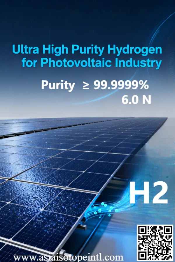
Power Electronics: Wide-bandgap semiconductors like silicon carbide and gallium nitride for power applications require ultra-pure process gases to achieve theoretical performance limits.
Emerging Purification Technologies
Several innovative approaches show promise for achieving even higher purity levels:
Electrochemical Hydrogen Pumping: Using proton-conducting membranes to selectively transport hydrogen ions while rejecting all impurities.
Getter-Based Purification: Employing reactive metal alloys that chemically bind impurities while allowing hydrogen to pass freely.
Plasma-Based Purification: Using non-equilibrium plasmas to selectively dissociate and remove molecular impurities.
Sustainability Considerations
The semiconductor industry increasingly emphasizes environmental sustainability, driving innovations in hydrogen production and purification:
Green Hydrogen: Producing hydrogen through water electrolysis powered by renewable energy sources eliminates carbon emissions associated with traditional steam methane reforming.
Recovery and Recycling: Advanced membrane systems allow recovery and purification of hydrogen from process exhaust streams, reducing consumption and waste.
Energy Optimization: Heat integration and process optimization reduce the energy footprint of purification systems while maintaining purity standards.
Conclusion: The Foundation of Tomorrow’s Technology
The remarkable purity of 6N hydrogen represents far more than a technical specification—it embodies the semiconductor industry’s relentless pursuit of perfection. Every additional nine in purity specification reflects years of research, millions of dollars in development, and breakthrough innovations in separation science.
As we stand on the threshold of revolutionary technologies—artificial intelligence, quantum computing, autonomous vehicles, and beyond—the demand for ultra-pure hydrogen will only intensify. The invisible flow of 6N hydrogen through semiconductor fabs worldwide enables the visible transformation of our digital society.
For those of us who have dedicated our careers to advancing specialty gas technology, the achievement of 6N purity in industrial-scale production represents a triumph of human ingenuity. Yet we recognize this is not the endpoint but rather a milestone on the continuing journey toward ever-greater purity and precision.
The next time you use a smartphone, drive a modern car, or benefit from medical diagnostics, remember that these technologies rest upon a foundation of extraordinary purity—where success is measured not by what is present, but by what has been meticulously removed. In the realm of semiconductor manufacturing, 6N hydrogen isn’t just a gold standard; it’s the invisible enabler of our technological future.
Would you like a deeper dive into any specific technical parameters or applications?
As an industry leader focused in Specialty Gases products, our goal is to support our customers by keeping them at the forefront of their industries. We’re here to help with any questions you might have so you can transform your ideas into reality, and tackle those big science challenges.
Get free consultant, our experts are ready to serve.
(Follow up our update articles on www.asiaisotopeintl.com or send your comments to tao.hu@asiaisotope.com for further communications)