Ultra High Purity Hydrogen (UHP H2): The Cornerstone of Advanced Semiconductor and Optical Fiber Manufacturing
BY Tao, Published Jan 5, 2026
In the global technology ecosystem, we often fixate on the visible hardware: the gleaming silicon wafers, the intricate processors inside our smartphones, and the thousands of miles of cabling that form the backbone of the internet. Yet, as China Isotope Development Co Ltd was starting to supply Ultra High Purity Hydrogen (UHP H2) to China domestic clients, I can tell you that the true magic happens at the molecular level.
At the center of this microscopic universe sits a single element, deceptively simple yet industrially demanding: Hydrogen ().
To the general public, hydrogen is the fuel of the future. To the semiconductor and optical fiber engineer, it is the tool of the present. But we are not talking about standard industrial hydrogen. We are talking about Ultra High Purity (UHP) Hydrogen—gas refined to such an extreme degree that “purity” is measured not in percentages, but in parts per trillion (ppt).
Today, I want to take you deep into the world of UHP Hydrogen. We will explore why it is the non-negotiable cornerstone of the Angstrom-era chip manufacturing and the silent guardian of global data transmission.
1. Defining “Ultra High Purity” in a Nano-Scale World
Before we discuss applications, we must establish a baseline for what “purity” means in our field.
In standard industrial applications (like steel refining or basic chemical synthesis), “Four Nines” (99.99%) purity is acceptable. In the fuel cell vehicle market, we strive for “Five Nines” (99.999%).
However, in the world of 3-nanometer semiconductor nodes, 99.999% purity is effectively “dirty.” It would destroy a modern fab’s yield instantly.
For advanced electronics and optical fibers, we deal in “Nine Nines” (99.9999999%). To visualize this, imagine a chain of 1 billion people standing hand-in-hand, wrapping around the earth multiple times. If this chain represented UHP Hydrogen, only one person in that entire line would be an impurity (like an oxygen or moisture molecule).
The “Killer” Impurities
Why such obsession with purity? Because at the atomic scale, specific impurities act as saboteurs:
- Moisture (𝐻2𝑂): The arch-enemy. It creates oxides on silicon surfaces, increasing electrical resistance and causing “black loss” in optical fibers.
- Hydrocarbons (𝐶𝑥𝐻𝑦): These introduce unwanted carbon atoms, altering the electrical doping profile of a chip.
- Particulates: Any solid particle larger than 10 nanometers can short-circuit a transistor that is only 20 nanometers wide.
Now, let us examine how this gas drives our most critical industries.
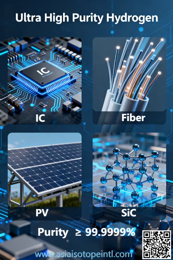
2. The Semiconductor Ecosystem: Hydrogen as the “Reductive Architect”
In a semiconductor fabrication plant (Fab), Hydrogen is omnipresent. It is used in dozens of steps, but its role changes depending on the process. I categorize its function into three pillars: Epitaxy, Annealing, and Lithography.
A. Epitaxy: The Carrier and the Cleaner
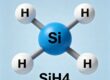
Epitaxy is the process of growing a perfect crystalline layer on top of a wafer. This is the canvas upon which the chip is built. In Silicon (Si) and Silicon Carbide (SiC) epitaxy, Hydrogen acts as the carrier gas. It transports the silicon source chemicals (like Trichlorosilane or Silane) into the reactor.
But it does more than carry. Hydrogen creates a reducing atmosphere.
- The Mechanism: At temperatures over 1000°C, Hydrogen actively strips away native oxygen from the wafer surface (𝑆𝑖𝑂2+𝐻2→𝑆𝑖+𝐻2𝑂). This ensures the new crystal layer hits a pristine, atom-perfect surface. If the Hydrogen contains even trace amounts of moisture (oxygen), the crystal will grow with defects, ruining the chip.
B. Annealing: Healing the Crystal
After we bombard a wafer with ions to create electrical pathways (Ion Implantation), the silicon crystal structure is damaged. It looks like a bombed-out city at the atomic level. We must repair this through Annealing—baking the wafer at high heat. Here, UHP Hydrogen is used to penetrate the lattice. It bonds with “dangling bonds” (broken silicon atoms), essentially healing the electrical flaws. This drastically improves the performance and reliability of the transistor.
C. EUV Lithography: The New Frontier
This is perhaps the most cutting-edge application. Modern chips (7nm and below) are made using Extreme Ultraviolet (EUV) Lithography. EUV machines generate light by blasting molten tin droplets with a laser. This creates a messy environment of tin debris.
- The Solution: We inject low-pressure Hydrogen gas into the EUV chamber. The high-energy EUV light turns the Hydrogen into a plasma. This hydrogen plasma reacts with the tin debris, turning it into a gas (Stannane, 𝑆𝑛𝐻4) that can be pumped away.
- The Purity Demand: In this vacuum environment, any impurity in the hydrogen would absorb the precious EUV light, reducing the machine’s efficiency. Therefore, EUV requires the absolute highest grade of hydrogen available to man.
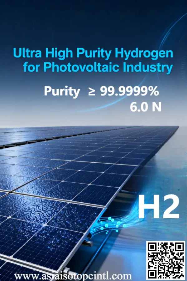
3. Optical Fiber Manufacturing: The Battle Against Attenuation
While semiconductors process data, optical fibers move it. The manufacturing of optical fiber preforms (the large glass rods that are drawn into thin fibers) is a masterclass in gas chemistry.
The core of an optical fiber is made of ultra-pure silica (). To make this, we burn silicon tetrachloride () in a hydrogen-oxygen flame. This process is called Hydrolysis.
The “Water Peak” Phenomenon
You might ask: “If we burn Hydrogen to make water vapor in the process, why does the Hydrogen need to be dry?”
It is a paradox, but a critical one. In the manufacturing of “Low Water Peak” fibers (the standard for modern telecommunications), we must avoid the formation of Hydroxyl (OH-) ions inside the glass structure.
- The Physics: The OH- bond vibrates at a specific frequency. Unfortunately, this vibration absorbs light exactly at the 1383 nm wavelength—a crucial window for data transmission. This absorption is called “Attenuation.”
If the incoming Hydrogen fuel contains hydrocarbon impurities or pre-existing moisture, it disrupts the precise stoichiometry of the flame, embedding excess OH- ions into the glass.
- The Consequence: The fiber becomes “blind” in certain spectrums, requiring more amplifiers across the ocean floor, costing telecom companies millions.
- The Expert View: By using UHP Hydrogen (free of hydrocarbons), we control the combustion reaction so precisely that we can virtually eliminate the water peak, allowing data to flow unhindered for hundreds of kilometers.
4. The Technology of Purification: How We Achieve 9N
Generating Hydrogen is easy; purifying it to 9N is an engineering marvel. As a specialist, I often guide clients through the selection of purification technologies. There are two primary methods used in the high-tech supply chain.
A. The Palladium Membrane: The Ultimate Filter
For the most critical applications (like EUV or SiC Epitaxy), we rely on Palladium Diffusion. Palladium is a rare metal with a unique property: when heated to roughly 300-400°C, its atomic lattice expands just enough to let Hydrogen nuclei (protons) pass through, but nothing else.
- The Analogy: Imagine a net where the holes are so small only a single marble can pass, but a bowling ball (Oxygen or Nitrogen) is blocked.
- The Result: The gas exiting a palladium cell is chemically perfect. It is the gold standard for purity.
B. Getter-Based Purification
For high-volume, bulk supply where palladium is too expensive or restrictive (palladium restricts flow rates), we use Getter columns. These are large vessels filled with beads of zirconium-vanadium-iron alloys. These alloys act like chemical sponges.
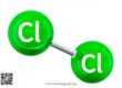
- Mechanism: They operate on the principle of Chemisorption. Impurities like , , and form irreversible chemical bonds with the alloy surface. The Hydrogen flows past, untouched.
- Evolution: Modern getters work at ambient temperatures, making them energy-efficient for large-scale LED or memory fabs.
5. Metrology: Measuring the Invisible
You cannot manage what you cannot measure. One of the biggest challenges in my field is proving that the gas is actually 99.9999999% pure. Standard sensors fail at this level.
We utilize a technology called APIMS (Atmospheric Pressure Ionization Mass Spectrometry) or CRDS (Cavity Ring-Down Spectroscopy).
- CRDS Explained: This is a fascinating technique. We trap a laser pulse between two highly reflective mirrors inside a cavity filled with the hydrogen sample. The light bounces back and forth kilometers of distance.
- If a moisture molecule is present, it absorbs a tiny fraction of that light. By measuring how fast the light intensity decays (“rings down”), we can calculate the exact concentration of moisture down to parts per trillion.
This level of metrology is what separates a standard gas supplier from a semiconductor-grade partner.
6. Safety and Material Science: The Hydrogen Embrittlement Challenge
No article on Hydrogen is complete without addressing safety, but from a materials engineering perspective.
High-pressure Hydrogen has a nasty habit: it attacks metal. This is called Hydrogen Embrittlement. Hydrogen atoms are so small they diffuse into the steel walls of pipes and tanks. They collect in the grain boundaries of the metal, creating internal pressure that eventually causes the steel to crack and shatter catastrophically.
The Solution: In UHP systems, we cannot use standard steel. We use:
- 316L Stainless Steel: The “L” stands for Low Carbon. Less carbon means fewer sites for hydrogen to attack.
- Electropolishing (EP): We electrically strip the inner surface of the pipes to a mirror finish. This removes microscopic cracks where hydrogen could enter the metal, and also removes surface area where moisture could hide.
7. The Future: Green Hydrogen in High-Tech?
As the world pivots to Green Hydrogen (produced via electrolysis using renewable energy), the high-tech industry faces a dilemma. Electrolysis produces Hydrogen by splitting water. Consequently, the output is extremely “wet” (saturated with moisture) and often contains traces of Oxygen.
For a fuel cell bus, this is fine. For a semiconductor fab, it is a contamination nightmare. The challenge for the next decade will be integrating Green Hydrogen sources with advanced, on-site purification systems that can handle the high moisture load and convert it into the 9N dry gas required for chip fabrication. This “Point-of-Use” purification strategy will be vital for fabs looking to lower their carbon footprint without sacrificing yield.
8. Conclusion
Hydrogen is often the smallest molecule in the room, but it carries the heaviest burden in modern manufacturing.
Whether it is acting as the reductive atmosphere that allows a 3nm transistor to form, the cleaning plasma in an EUV machine, or the fuel that creates the glass for the internet, Ultra High Purity Hydrogen is the invisible thread connecting our digital world.
For industry leaders, investors, and engineers, understanding the nuance of UHP gas is not just chemistry—it is business strategy. In the race for faster chips and clearer signals, purity is not a luxury; it is the fundamental limit of what is possible.
Would you like a deeper dive into any specific technical parameters or applications?
As an industry leader focused in Specialty Gases products, our goal is to support our customers by keeping them at the forefront of their industries. We’re here to help with any questions you might have so you can transform your ideas into reality, and tackle those big science challenges.
Get free consultant, our experts are ready to serve.
(Follow up our update articles on www.asiaisotopeintl.com or send your comments to tao.hu@asiaisotope.com for further communications)