The Next Frontier: Unlocking Silicon Carbide (SiC) Potential with Ultra High Purity Hydrogen Technology
BY Tao, Published Jan 5, 2026
The global electronics landscape is undergoing a seismic shift. As we race toward a carbon-neutral future, the demand for power efficiency has never been more critical. At the heart of this transformation lies Silicon Carbide (SiC), a wide-bandgap semiconductor that promises to redefine the limits of power electronics, from Electric Vehicles (EVs) to renewable energy grids.
However, as China Isotope Development Co Ltd was starting to supply Ultra High Purity Hydrogen (UHP H2) , I see a recurring bottleneck. The industry often focuses heavily on the lithography and packaging of these chips, yet frequently overlooks the invisible backbone of the entire process: Ultra High Purity (UHP) Gases.
Specifically, the role of UHP Hydrogen () in SiC epitaxy is the single most critical variable in determining whether a wafer yields a high-performance chip or becomes expensive scrap. Today, we will explore why unlocking the full potential of SiC is impossible without mastering the chemistry of Ultra High Purity Hydrogen.
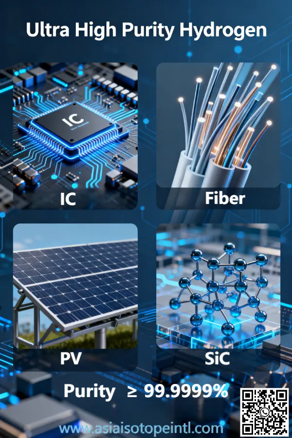
Ultra High Purity Hydrogen UHP H2
1. The Silicon Carbide Revolution: Why Now?
To understand the gas requirements, we must first understand the material. For decades, traditional Silicon (Si) was the king of semiconductors. But in high-power applications, Silicon hits a physical wall.
Silicon Carbide is often called a “Wide Bandgap” material. To put it simply, imagine a dam holding back water (electricity). Traditional Silicon is like a standard concrete dam—effective, but if the pressure (voltage) gets too high, it cracks. SiC is like a diamond-reinforced steel dam; it can withstand roughly 10 times the breakdown field strength of silicon.
This allows SiC chips to:
- Operate at much higher voltages (HV).
- Switch on and off at incredible speeds (high frequency).
- Endure extreme heat (thermal conductivity).
This trilogy of benefits is why Tesla, BYD, and major grid operators are transitioning to SiC. However, growing SiC crystals is notoriously difficult. Unlike silicon, which is grown from a melt, SiC is grown via vapor phase epitaxy. This is where the gas experts step in.
2. The Invisible Backbone: Epitaxy and the Role of Hydrogen
The manufacturing of SiC relies heavily on a process called Chemical Vapor Deposition (CVD), specifically during the Epitaxy (Epi) phase.
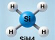
In this process, we grow a thin, perfect crystalline layer on top of a base SiC wafer. This layer is where the electricity will actually flow. To grow this layer, we inject silicon-containing gases (like Silane) and carbon-containing gases (like Propane) into a reactor heated to over 1600°C.
So, where does Hydrogen fit in?
Hydrogen is not just a passive carrier gas that pushes these ingredients into the chamber. In the high-temperature world of SiC epitaxy, Hydrogen is an active chemical reagent. It performs three distinct, critical functions:
- Carrier Medium: It transports the precursor chemicals (Silane/Propane) uniformly across the wafer.
- Surface Etching (Cleaning): Before growth begins, Hydrogen attacks the surface of the wafer to strip away oxides and impurities. It “scrubs” the floor before we lay the new tile.
- Step-Flow Control: This is the most technical aspect. SiC grows in “steps” (think of a microscopic staircase). Hydrogen dictates the surface chemistry, ensuring the atoms settle in the right order. If the hydrogen chemistry is off, the steps bunch up (Step Bunching), creating rough surfaces and defective chips.
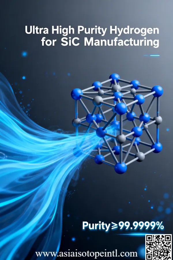
3. Defining “Ultra High Purity” in the SiC Context
In the industrial gas world, we talk about “Nines.” Standard industrial hydrogen might be 99.99% pure (4N). For a forklift fuel cell, that is excellent. For a Silicon Carbide wafer, that is catastrophic.
For SiC Epitaxy, we are looking at 7N (99.99999%) or even 9N purity levels at the point of use. But the total purity percentage is less important than the specific impurities hidden within that remaining fraction.
As a specialist, I track three “Killer Impurities” that must be controlled at the parts-per-billion (ppb) level:
A. Moisture () and Oxygen ()
This is the arch-enemy of SiC. If oxygen is present during the growth phase, it oxidizes the surface.
- The Impact: It creates “nucleation sites”—basically, small bumps that ruin the crystal structure. It can lead to triangular defects and “downfall” particles.
- The Threshold: We aim for moisture levels below 0.5 ppb (parts per billion). To visualize this, that is equivalent to half a drop of water in an Olympic-sized swimming pool.
B. Hydrocarbons (, etc.)
Since SiC is made of Silicon and Carbon, you might think extra carbon in the hydrogen supply is fine. It is not.
- The Impact: The ratio of Carbon to Silicon (C/Si Ratio) in the reactor must be precise to the decimal point. Uncontrolled hydrocarbons from the hydrogen supply throw this ratio off balance, altering the “doping concentration” (the chip’s electrical conductivity).
C. Nitrogen ()
Nitrogen is a “dopant” for SiC, meaning it changes how the material conducts electricity.
- The Impact: If your hydrogen has trace nitrogen, you are essentially unintentionally doping your chip, making it conductive when it should be resistive, or altering its breakdown voltage.
4. The Mechanism: How Impurity Control Boosts Yield
Let’s look at the mechanism of action. Why does investing in ultra-pure hydrogen technology translate to business success? It comes down to Yield.
In the semiconductor industry, “Yield” is the percentage of chips on a wafer that actually work. Currently, SiC yields are lower than traditional silicon because the material is prone to defects like Basal Plane Dislocations (BPDs) and Micro-pipes.
When we utilize UHP Hydrogen technology, we influence the “Step-Flow” growth mode.
The “Step-Flow” Analogy: Imagine laying bricks to build a wall. If you lay them perfectly flat, the wall is strong. If you have dust (impurities) on the layer beneath, the next brick tilts slightly. Ten layers up, that tilt becomes a massive crack. In SiC, UHP Hydrogen ensures the atomic “bricks” flow smoothly to the edge of the atomic “step.” It stabilizes the surface energy.
Real-world Data: Research and fab data suggest that improving hydrogen purity from 6N to 8N/9N, specifically by removing moisture and nitrogen spikes, can reduce epitaxial defect density by 15% to 20%. In an industry where a single 150mm SiC wafer costs thousands of dollars, that efficiency gain is worth millions annually.
5. Technical Challenges in the UHP Hydrogen Supply Chain
Achieving this level of purity is not about simply buying a better tank of gas. It requires a holistic approach to the Gas Delivery System (GDS). As an expert, I advise clients to look at the “Three Pillars of Purity”:
1. Purification Technology
Standard Pressure Swing Adsorption (PSA) is rarely enough for the final stage. The gold standard for SiC Hydrogen is Palladium Diffusion.
- How it works: Palladium is a unique metal. When heated, it acts like a sponge that only allows Hydrogen atoms to pass through its lattice structure. Every other molecule (oxygen, moisture, nitrogen) is too big and gets blocked.
- The Result: The hydrogen emerging from a palladium membrane is theoretically purity-perfect (99.9999999%).
2. The “Getter” Systems
For high-volume fabs where palladium might be too flow-restrictive, we use advanced Getter purifiers. These are vessels filled with zirconium-based alloys that chemically react with impurities, trapping them permanently.
- Expert Tip: Many fabs fail here because they do not monitor the “breakthrough” point—the moment the purifier is full. Redundant monitoring is essential.
3. Stainless Steel Electropolishing
You can generate perfect hydrogen, but if your pipes are dirty, it doesn’t matter. We use 316L Stainless Steel with Electropolished (EP) inner surfaces.
- Why? Standard steel has microscopic rough peaks and valleys that trap moisture. Electropolishing smooths the steel to a mirror finish, ensuring that moisture has nowhere to hide and can be easily purged.
6. The Transition to 200mm (8-inch) Wafers
The industry is currently migrating from 150mm (6-inch) to 200mm (8-inch) wafers to reduce costs. This transition drastically increases the difficulty of the process.
On a larger wafer, uniformity is harder to maintain. The gas flow dynamics change. If the Hydrogen carries even a microscopic amount of impurity, the defect distribution across a 200mm surface becomes more pronounced, specifically at the wafer edges.
UHP Hydrogen technology becomes even more vital here. The larger the surface area, the higher the probability of a “killer defect” landing on a critical part of the chip. Therefore, as fabs move to 200mm, the tolerance for gas impurities drops effectively to zero.
7. Future Outlook: The Green Hydrogen Synergy
Looking ahead, there is an interesting convergence between the Green Hydrogen economy and the Semiconductor industry.
Currently, most UHP Hydrogen is derived from fossil fuels (Steam Methane Reforming) and then heavily purified. However, as electrolysis technology (splitting water with renewable energy) improves, we are seeing the potential for on-site Green Hydrogen generation.
The challenge? Electrolysis produces “wet” hydrogen (saturated with moisture). This brings us back to purification. The future of SiC manufacturing will likely involve on-site electrolyzers coupled with advanced Palladium purifiers, creating a closed-loop, sustainable, and ultra-pure supply chain.
8. Conclusion: Purity as a Strategic Asset
In summary, Silicon Carbide is the engine of the modern power revolution, but Ultra High Purity Hydrogen is the fuel that keeps that engine running without seizing.
For manufacturers, the investment in UHP hydrogen technology—purifiers, electropolished piping, and trace analyzers—should not be viewed as a utility cost. It is a strategic asset. It is the lever that lifts yield rates, improves device reliability, and ultimately lowers the cost per amp for the end user.
As we push the boundaries of voltage and efficiency, the difference between success and failure will increasingly be measured not in percent, but in parts per billion.
Would you like a deeper dive into any specific technical parameters or applications?
As an industry leader focused in Specialty Gases products, our goal is to support our customers by keeping them at the forefront of their industries. We’re here to help with any questions you might have so you can transform your ideas into reality, and tackle those big science challenges.
Get free consultant, our experts are ready to serve.
(Follow up our update articles on www.asiaisotopeintl.com or send your comments to tao.hu@asiaisotope.com for further communications)