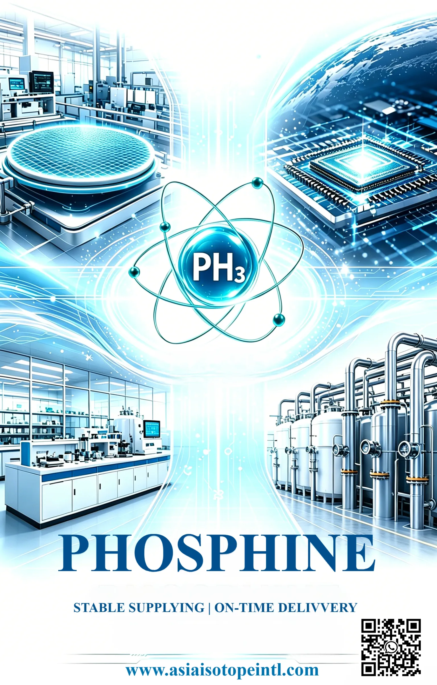
Beyond Doping: How Phosphine (PH3) Is Powering the Next Generation of
Quantum Dots and Optoelectronics
BY Eve, Published July 4, 2026
For decades, phosphine (PH3) has been the invisible workhorse of the semiconductor industry—a simple, highly toxic gas that serves as the primary source of phosphorus for doping silicon wafers. Yet in recent years, this unassuming molecule has quietly expanded its repertoire far beyond conventional ion implantation. Today, high-purity phosphine is at the heart of some of the most exciting frontiers in materials science: colloidal quantum dots with near-unity quantum yields, cadmium-free displays that rival OLEDs in performance, and next-generation optoelectronic devices that promise to reshape how we generate and manipulate light.
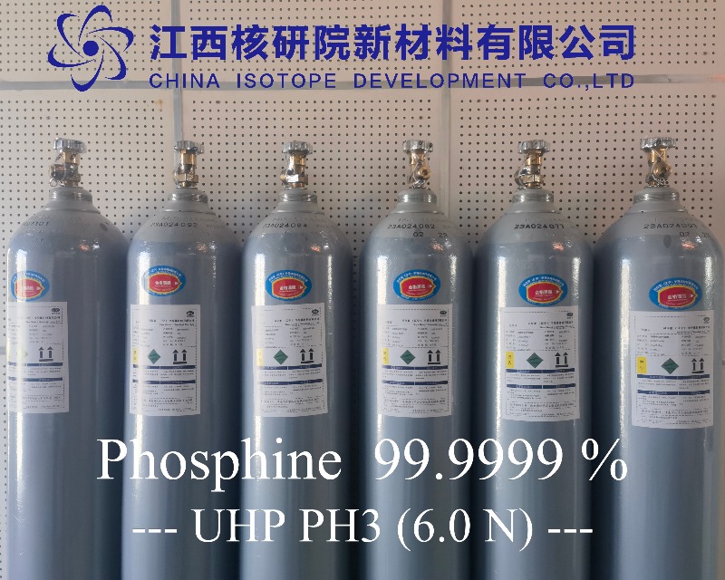
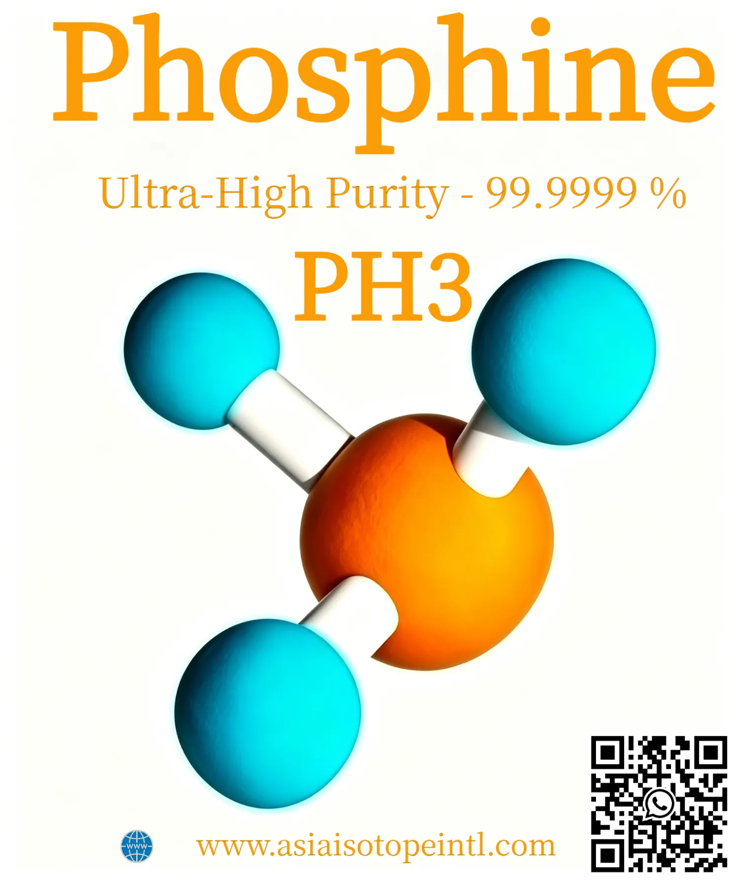
This transformation is not merely incremental. It represents a fundamental shift in how the electronics industry thinks about phosphorus chemistry—moving from bulk doping of planar silicon to atomic-scale engineering of nanostructured materials with precisely tunable optical and electronic properties. And at the center of this revolution stands electronic-grade phosphine, purity 99.999% and above. China Isotope Development Co Ltd supply high purity Phosphine (PH3) up to 99.9999% (6N) and higher, depending on customer requirements. As the professional supplier, China Isotope Development maintain strict quality control for consistent purity with very low levels of impurities such as oxygen, moisture, and hydrocarbons, to meet client high tech requirements.
1. From Planar Doping to 3D Nanostructures
1.1 The Limitations of Traditional Ion Implantation
The semiconductor industry’s insatiable demand for higher performance and lower power consumption has driven transistor architectures to unprecedented levels of complexity. Traditional ion implantation, while effective for planar devices, struggles to deliver conformal doping in three-dimensional structures such as FinFETs, nanowires, and gate-all-around (GAA) transistors.
1.2 Phosphine-Based Vapor-Phase Doping
Phosphine offers a compelling alternative. Through vapor-phase doping processes conducted at or near atmospheric pressure, PH₃ can penetrate the narrowest recesses of 3D silicon structures with minimal lattice damage. This approach is particularly promising for GAA nanowire devices, where conformal doping of source/drain regions is essential for maintaining consistent electrical properties.
1.3 Advancements in SiGe Alloy Doping
Recent research has demonstrated that phosphine-based doping of silicon-germanium alloys (Si₁₋ₓGeₓ:P) can achieve both improved surface morphology and increased active carrier concentrations at lower growth temperatures. This capability is critical for the thermal budget constraints of advanced nodes, where excessive heat can degrade device performance through unwanted diffusion. In-situ doping during nanowire growth—introducing PH₃ gas precursors during silicon and germanium nanowire growth—has emerged as a particularly effective strategy.
| Application | Role of Phosphine | Key Advantage |
|---|---|---|
| FinFET Doping | N-type dopant source | Conformal doping of 3D structures |
| GAA Nanowire Doping | Vapor-phase PH₃ delivery | Minimal lattice damage, shallow junctions |
| SiGe Alloy Doping | PH₃-based doping | Improved surface morphology |
| MLD (Monolayer Doping) | Ultrashallow doping source | No crystal damage, 3D structure compatibility |
1.4 Market Momentum
The scale of this demand is reflected in market projections. The global phosphine gas market in semiconductor applications was valued at approximately US$78 million in 2024 and is expected to reach US$128 million by 2031, growing at a compound annual rate of 7.0%. Electronic-grade phosphine (6N purity) accounts for an overwhelming 88% of this market, underscoring the industry’s relentless drive toward higher purity. With the expansion of 5G networks, IoT devices, artificial intelligence, and advanced computing, this trajectory shows no signs of slowing.
2. The Quantum Dot Revolution
2.1 Indium Phosphide Quantum Dots as a Cadmium-Free Alternative
Perhaps the most visually striking application of phosphine lies in the synthesis of colloidal quantum dots (QDs)—nanoscale semiconductor crystals whose optical properties can be precisely tuned by controlling their size. Among these, indium phosphide (InP) quantum dots have emerged as the leading cadmium-free alternative for display applications, driven by increasingly stringent environmental regulations in Europe and Asia.
2.2 Phosphine as the Critical Phosphorus Precursor
Phosphine serves as the critical phosphorus precursor in InP QD synthesis. The chemistry is elegant but demanding: PH₃ must be generated in situ or delivered with exquisite control to achieve the monodisperse particle distributions essential for high-performance devices. Recent advances in aminophosphane precursors have improved atomic efficiency, though challenges remain with byproduct formation. Alkylsilylamine-based aminophosphine precursors have been newly introduced to address these limitations.
2.3 Breakthrough Performance Metrics
The results, however, are extraordinary. Researchers have achieved green-emitting InP/ZnSe/ZnS quantum dots with photoluminescence quantum yields exceeding 90% using tris(diethylamino)phosphine as the phosphorus source. Blue-emitting CsPbBr₃ quantum dots passivated with phosphine ligands have reached near-unity quantum yields of 97.9%. These performance metrics place InP-based QDs on a competitive footing with their cadmium-containing counterparts—without the associated toxicity concerns.
2.4 Commercial Impact and Display Applications
The commercial implications are profound. Phosphine-based QDs are already finding their way into high-end displays, where their narrow emission spectra and high color purity enable wider color gamuts and improved energy efficiency. Direct ambient photopatterning of RGB quantum dots using triphenylphosphine—a molecule that functions simultaneously as a surface ligand, photoinitiator, and oxidation protector—has enabled light-emitting diodes with external quantum efficiencies exceeding 20%. Acylphosphines have also emerged as solid-state, non-pyrophoric, and synthetically accessible phosphorus precursors for InP nanocrystal synthesis.
3. Phosphine in Photovoltaics: Pushing Efficiency Boundaries
3.1 Role of PH3 in Silicon Heterojunction Solar Cells
The solar energy sector represents another rapidly growing frontier for phosphine applications. In silicon heterojunction (SHJ) solar cells, phosphine gas flow fraction (f PH₃) plays a decisive role in determining the optoelectronic properties of n-type nanocrystalline silicon oxide (nc-SiOₓ:H) window layers.
3.2 Systematic Characterization and Performance Optimization
Systematic characterization has revealed that the PH₃ gas fraction governs not only phosphorus doping efficiency but also the microstructure, oxygen content, and crystalline phase of the films. At moderate f PH₃ values, researchers achieved a remarkable conductivity of 2.84 × 10⁻¹ S/cm with an optical band gap of 2.26 eV—parameters that translated into solar cell efficiencies of 23.7%.
3.3 Record Efficiencies and the Path to Theoretical Limits
The push for ever-higher efficiency continues. Silicon heterojunction cells have recently achieved certified record efficiencies of 27.30%, bringing these technologies closer to their theoretical limit of 29.5%. Perovskite/silicon tandem solar cells have reached 34.6% efficiency, further expanding the potential application space for phosphine-based doping technologies.
3.4 Emerging Photovoltaic Technologies
Beyond silicon-based devices, phosphine is finding applications in emerging photovoltaic technologies. Organophosphorus compounds have been used to dope single-walled carbon nanotube films for inverted perovskite solar cells, boosting device efficiency from 5.1% to 8.03%. Phosphine oxide-based interfacial modifiers have pushed wide-bandgap perovskite solar cells to power conversion efficiencies of 21.0%. These developments suggest that phosphine chemistry will remain central to photovoltaic research for years to come.
4. Gas Sensing: Protecting Lives with Advanced Materials
4.1 The Toxicity Imperative
The very toxicity that makes phosphine so valuable in semiconductor processing also makes it a significant safety concern. Phosphine is a colorless, highly toxic, and flammable gas with a garlic-like or fishy odor. It can ignite spontaneously on contact with air. Exposure can cause severe respiratory disorders, pulmonary edema, and even death.
4.2 The Push for Highly Sensitive Detection
This duality—indispensable yet dangerous—has driven extensive research into phosphine gas sensors. The need for highly sensitive and selective detection methods has spurred investigation into novel nanomaterials. Density functional theory (DFT) studies have explored various two-dimensional materials as potential PH₃ sensing platforms.
4.3 Borophene-Based Sensing Platforms
Borophene nanosheets have been investigated as a promising base material for selective chemical sensors and molecular capture platforms aimed at dangerous gases like phosphine. DFT simulations have analyzed different adsorption sites and molecular configurations, evaluating adsorption energy to determine optimal sensing performance.
4.4 Graphene, h-BN, and Arsenene Nanoribbons
Graphene nanosheets, both pristine and doped, have been studied extensively for their adsorption and sensing properties in interaction with phosphine gas. Transition metal doping of hexagonal boron nitride (h-BN) nanosheets has shown significant enhancement of PH₃ detection capacity. Hydrogenated armchair and zigzag arsenene nanoribbons have been identified as potential platforms for detecting PH₃ gas molecules, with resistance variation upon adsorption serving as the detection mechanism.
4.5 From Computation to Commercial Reality
These computational predictions are increasingly being validated by experimental work, bringing practical PH₃ sensors closer to commercial reality.
5. Environmental Remediation: From Toxic Gas to Valuable Resource
5.1 A Paradigm Shift in Abatement Strategies
The environmental dimension of phosphine chemistry is undergoing a remarkable transformation. Historically, phosphine abatement focused on simply removing the toxic gas from industrial emissions through adsorption, catalytic decomposition, or plasma treatment. Today, researchers are pursuing a more ambitious vision: converting captured phosphine into valuable resources.
5.2 CuCe Co-Doped Biochar Adsorbents
Recent breakthroughs include CuCe co-doped nitrogen-rich biochar adsorbents that achieve PH₃ breakthrough capacities of 152.6 mg·g⁻¹ at 60 °C under anaerobic conditions. What makes this approach remarkable is what happens next: the spent adsorbent, now containing phosphorus-rich Cu₃P, exhibits exceptional supercapacitor performance with specific capacitance of 450.60 F·g⁻¹. This “waste-to-wealth” strategy transforms an environmental liability into an energy storage asset.
5.3 CuO@NC and NiO/TiO₂ Sorbents
Similarly, novel CuO@NC sorbents synthesized via direct thermal treatment of urea and copper nitrate have demonstrated efficient PH₃ purification at temperatures as low as 90 °C, with a capacity of 272.54 mg g⁻¹, offering the added benefit of Cu₃P resource recovery. NiO/TiO₂ adsorbents have achieved even higher breakthrough capacities of 232.23 mg(PH₃) g⁻¹ at 350 °C.
| Sorbent Material | Operating Temperature | Capacity (mg g⁻¹) | Value-Added Product |
|---|---|---|---|
| CuCe/N-rich Biochar | 60 °C | 152.6 | Cu₃P (supercapacitor electrode) |
| CuO@NC | 90 °C | 272.54 | Cu₃P (resource recovery) |
| NiO/TiO₂ | 350 °C | 232.23 | Photocatalytic degradation |
5.4 Toward Phosphorus Sustainability
These developments align with broader efforts toward phosphorus sustainability—an increasingly urgent concern given the finite nature of phosphate rock reserves. Cu-doped active carbon with nitrogen-modified stable active Cu²⁺ species has also been developed for efficient PH₃ removal, offering innovative approaches to catalyst design for phosphorus resource recovery.
6. Product Specifications and Quality Considerations
6.1 Purity Grades and Market Share
Electronic-grade phosphine is available in purities ranging from 99.999% (5N) to 99.9999% (6N) and beyond. The 6N grade accounts for approximately 88% of the semiconductor market segment. Total impurities are typically maintained below 1 ppm.
6.2 Key Impurity Species Monitored
Key impurity species monitored include moisture (H₂O), oxygen (O₂), carbon dioxide (CO₂), carbon monoxide (CO), methane (CH₄), and higher-order phosphines. The stringent purity requirements reflect the extreme sensitivity of advanced semiconductor processes to contamination—a single impurity atom can render an entire batch of devices defective.
6.3 Industry Standards and Chemical Properties
The industry standard specification is SEMI C3.6. Electronic-grade phosphine exhibits exceptional chemical properties essential for precision semiconductor doping applications, with ultra-pure composition and controlled chemistry ensuring reliable performance in demanding epitaxial growth processes.
6.4 Key Application Categories
Applications of high-purity phosphine can be broadly divided into:
-
Doping materials for converting silicon into n-type semiconductors
-
Raw materials for phosphorus-based compound semiconductors, including GaP and InP
6.5 Safety and Handling Requirements
Given its extreme toxicity and flammability, phosphine must be handled in dedicated gas cabinets with continuous leak monitoring, scrubbers, and emergency shutdown systems.
7. The Road Ahead
7.1 Converging Market Drivers
The phosphine market is entering a period of structurally elevated demand. Several converging trends are driving this growth: the expansion of GaN-on-Si power devices, the industrialization of advanced memory doping requirements, the scaling of compound semiconductor manufacturing, and the relentless push toward LED epitaxy innovation.
7.2 The LED Epitaxy Growth Engine
The LED epitaxy segment remains the largest consumer of phosphine precursor, driven by the transition from traditional LED to mini-LED and micro-LED architectures. Mini and micro-LED mass-transfer and epitaxy efficiency improvements are driving a 10–15% annual increase in MOCVD precursor demand within the LED segment, outstripping broader semiconductor materials growth.
7.3 Market Forecasts and Regional Landscape
Market forecasts project the global electronic-grade phosphine market growing from US$92.6 million in 2025 to US$145 million by 2032, representing a compound annual growth rate of 6.7%. Other estimates place the market at US$601.37 million in 2025, projected to reach US$1,035.27 million by 2032, reflecting the breadth of applications covered under broader definitions. The Asia-Pacific region dominates this market with approximately 80% share, followed by Europe and North America. Key players include Entegris, Linde plc, Versum Materials, Taiyo Nippon Sanso, and Solvay, with the top three holding over 80% of the market.
7.4 A Strategic Material for the Next Decade
As transistor dimensions continue to shrink toward atomic scales, as quantum dots find their way into an expanding array of display and lighting applications, and as photovoltaic technologies push toward their theoretical efficiency limits, the role of phosphine will only grow more central. This simple molecule—three hydrogen atoms bonded to a single phosphorus atom—has proven remarkably versatile, serving as both the foundation of modern electronics and a key enabler of the technologies that will define the next decade.
The journey of phosphine from a workaday dopant gas to a strategic material for advanced manufacturing is a testament to the creativity of materials scientists and process engineers. It is also a reminder that in the world of high-technology materials, the most valuable assets are often the ones we think we already understand—until we discover what else they can do.
Would you like a deeper dive into any specific technical parameters or applications?
As an industry leader focused in Specialty Gases , our goal is to support our customers by keeping them at the forefront of their industries. We’re here to help with any questions you might have so you can transform your ideas into reality, and tackle those big science challenges.
Get free consultant, our experts are ready to serve.
(Follow up our update articles on www.asiaisotopeintl.com or send your comments to tao.hu@asiaisotope.com for further communications)