Silane in Semiconductor Manufacturing: The Essential Precursor for CVD Thin‑Film Deposition
BY Eve, Published June 25, 2026
For nearly half a century, silane (SiH₄) has served as the foundational silicon source for the semiconductor industry. Since its introduction into semiconductor manufacturing in the late 1960s, this simple silicon hydride has become indispensable to the fabrication of virtually every integrated circuit produced today. When I reflect on the evolution of this industry—from the early days of micron‑scale geometries to today’s sub‑3nm nodes—few materials have demonstrated such enduring relevance. The reason is straightforward: silane offers a combination of thermal decomposition properties, purity scalability, and deposition versatility that no alternative silicon precursor has been able to fully replicate.
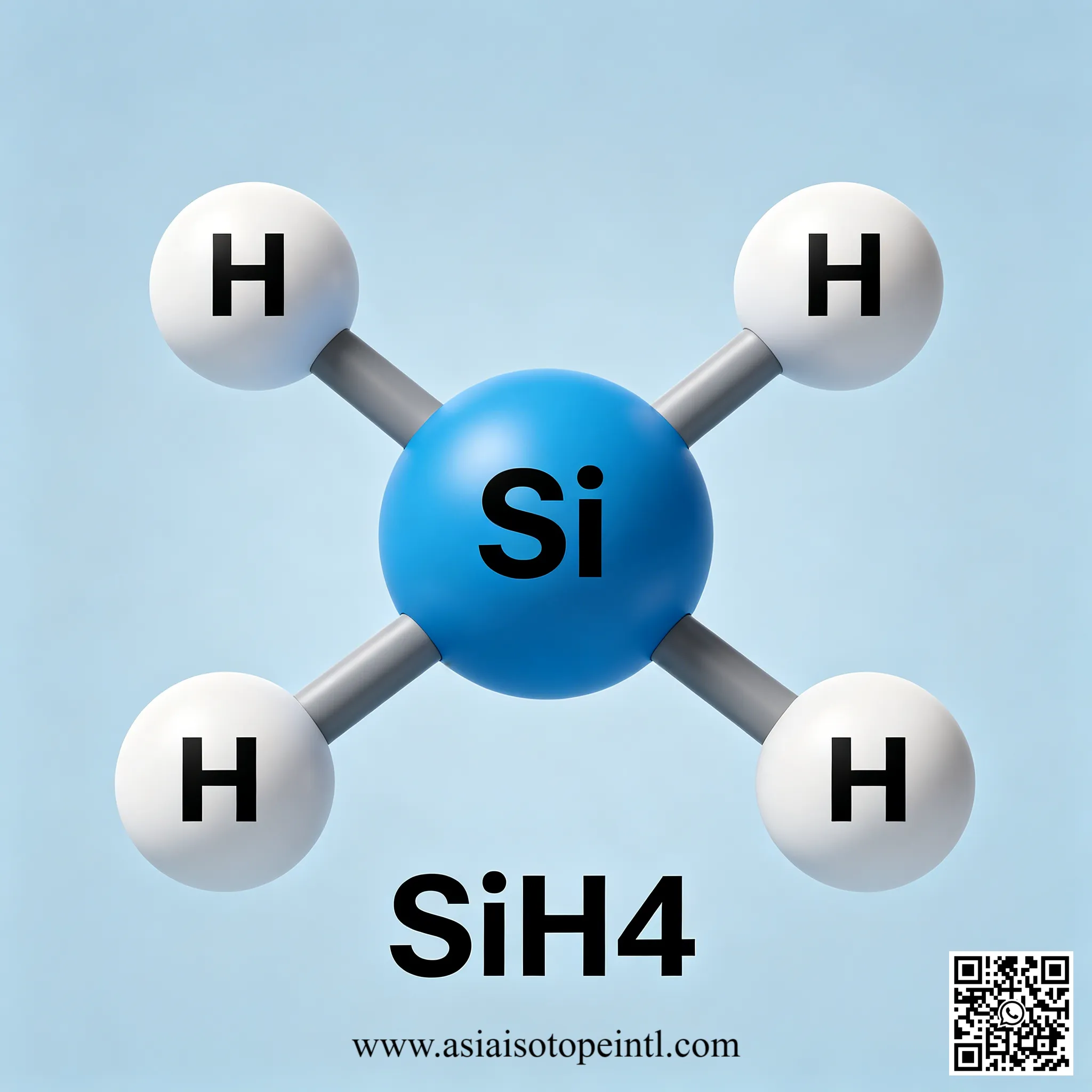
At its core, silane (CAS 7803‑62‑5) is the simplest silicon hydride, with a molecular weight of 32.117 g/mol and a boiling point of ‑112°C. At room temperature, it exists as a colorless, pyrophoric gas—meaning it ignites spontaneously upon exposure to air. This inherent reactivity, while demanding rigorous safety protocols, is precisely what makes silane so valuable. The compound undergoes complete thermal decomposition around 400°C, yielding elemental silicon and hydrogen gas. This decomposition temperature is significantly lower than that of alternative silicon sources such as dichlorosilane or trichlorosilane, enabling deposition processes at temperatures that are compatible with the thermal budgets of modern semiconductor fabrication.
Silane has become the most important special gas used in semiconductor microelectronics processes. It is used in the preparation of various microelectronic films, including monocrystalline film, microcrystalline, polycrystalline, silicon oxide, silicon nitride, and metal silicide. The microelectronic applications of silane continue to develop in depth, encompassing low‑temperature epitaxy, selective epitaxy, and heteroepitaxy—not only for silicon devices and silicon integrated circuits but also for compound semiconductor devices such as gallium arsenide and silicon carbide. Silane is used in almost all advanced integrated circuit production lines in modern times. China Isotope Development Co Ltd supply high purity silane up to 99.999% (5N) and higher, depending on customer requirements. As the professional supplier, China Isotope Development maintain strict quality control for consistent purity with very low levels of impurities such as oxygen, moisture, and hydrocarbons, to meet client high tech requirements.
1.The CVD Foundation: Why Silane Dominates Thin‑Film Deposition
Chemical vapor deposition (CVD) is the workhorse technique for building the layered structures of integrated circuits. The process involves introducing gaseous precursor molecules into a vacuum chamber, where they thermally decompose or react on the substrate surface to form a thin, uniform film. Silane’s role in this process is multifaceted and irreplaceable.
The fundamental reaction for silicon deposition from silane is straightforward: SiH₄ → Si + 2H₂. This decomposition is typically performed in low‑pressure CVD (LPCVD) systems, using either pure silane feedstock or silane diluted with nitrogen. The low‑pressure environment—typically in the range of 150 to 300 mTorr—ensures that the mean free path of reactant gases is sufficiently long to provide uniform gas distribution across the wafer surface. Under these conditions, the deposition operates in the “reaction rate limited regime,” where the deposition thickness becomes a linear function of time, enabling precise control over film thickness.
What distinguishes silane from alternative silicon sources is its decomposition behavior. Unlike chlorosilanes, which require higher temperatures and produce corrosive byproducts such as hydrogen chloride, silane decomposes cleanly to silicon and hydrogen. This clean decomposition pathway minimizes contamination risks and simplifies exhaust treatment. Moreover, silane enables epitaxial silicon growth rates approximately ten times higher than dichlorosilane at temperatures below 575°C, significantly reducing cost‑per‑wafer in high‑volume manufacturing.
2.Polycrystalline Silicon: The Workhorse of Semiconductor Devices
Polycrystalline silicon—commonly referred to as polysilicon or poly‑Si—represents one of the largest‑volume applications of silane in semiconductor manufacturing. Polysilicon films serve as the gate electrode material in MOS transistors, as the charge storage layer in floating‑gate memory devices, and as the structural material in MEMS devices.
The deposition of polysilicon from silane is typically performed in LPCVD furnaces at temperatures ranging from 560°C to 625°C. At these temperatures, silane pyrolyzes on the heated substrate surface, depositing a film of polycrystalline silicon. The deposition rate in a typical LPCVD process using silane is approximately 30 Å/min, with thickness uniformity across the wafer better than 1.5%.
One of the most significant advantages of silane‑based polysilicon deposition is the ability to perform in‑situ doping—that is, incorporating dopant atoms into the silicon film during deposition itself. By introducing phosphine (PH₃) for n‑type doping or diborane (B₂H₆) for p‑type doping into the CVD chamber alongside silane, manufacturers can produce doped polysilicon films in a single process step. This eliminates the need for separate ion implantation and annealing steps, reducing process complexity and thermal budget.
The standard recipe for phosphorus‑doped polysilicon deposition uses a silane flow of 150 sccm and a 1.5% PH₃/SiH₄ mixture flow of 40 sccm at 200 mTorr and 560–625°C. The resulting films exhibit electrical resistivity below 0.003 ohm‑cm. The temperature profile in the furnace is carefully tilted, with a higher value at the source end to compensate for silane depletion along the reactor tube due to the vacuum pump action.
In advanced 3D NAND flash memory manufacturing, polysilicon deposited from silane plays an even more critical role. The vertical channel holes in 3D NAND structures require conformal polysilicon deposition over extreme aspect ratios—a challenge that pushes the limits of conventional CVD and has driven the development of advanced deposition techniques.
3.Amorphous and Microcrystalline Silicon: Enabling Advanced Device Architectures
While polysilicon dominates logic and memory applications, hydrogenated amorphous silicon (a‑Si:H) and microcrystalline silicon (μc‑Si:H) have become essential materials for specific device architectures, particularly in display technology and advanced solar cell applications.
Amorphous silicon films are typically deposited by plasma‑enhanced chemical vapor deposition (PECVD) using silane. The plasma environment allows deposition at lower substrate temperatures—often below 300°C—making PECVD the method of choice when thermal budget constraints are severe. PECVD from silane is the most frequently used method for preparing a‑Si:H films. The hydrogen dilution of silane plays a crucial role in determining film quality. Strong dilution with hydrogen has been demonstrated to decrease the light‑induced degradation of a‑Si:H solar cells.
For thin‑film transistor (TFT) fabrication in LCD and OLED displays, silane serves as the silicon source for both the channel layer and the contact layers. The ability to deposit doped amorphous silicon layers—both n‑type and p‑type—by introducing phosphine or diborane into the PECVD chamber enables the fabrication of the transistor structures that drive each pixel in modern displays.
Microcrystalline silicon occupies an intermediate position between amorphous and crystalline silicon, offering higher charge carrier mobility than a‑Si:H while maintaining the low‑temperature deposition compatibility of PECVD. The transition from amorphous to microcrystalline silicon is achieved by increasing the hydrogen dilution of silane in the deposition process. The volume fraction of the microcrystalline phase depends strongly on the dilution ratio of silane gas. However, high hydrogen dilution typically results in low deposition rates—approximately 1 Å/s—which increases process time and production cost. This trade‑off between film quality and throughput has driven ongoing research into alternative deposition techniques such as hot‑wire CVD (HWCVD), where silane is dissociated over heated tungsten or tantalum filaments at temperatures above 1600°C.
4.Silicon Dioxide: The Insulating Backbone of Integrated Circuits
Silicon dioxide (SiO₂) is arguably the most important dielectric material in semiconductor manufacturing. It serves as the gate oxide in MOS transistors, as the isolation layer between metal interconnect lines, and as the masking material for selective doping and etching. Silane is one of the primary precursors for CVD silicon dioxide deposition.
The deposition of silicon dioxide from silane typically involves the reaction of silane with an oxygen source—most commonly oxygen (O₂) or nitrous oxide (N₂O). The reaction with oxygen proceeds as: SiH₄ + O₂ → SiO₂ + 2H₂. This reaction can be performed in conventional CVD systems at temperatures above 400°C, or in PECVD systems at lower temperatures using plasma enhancement.
One of the key advantages of silane‑based SiO₂ deposition is the ability to achieve good step coverage—the conformal coating of topography on the wafer surface. Silane oxidation has been found to result in approximately 70% device step conformality of silicon dioxide film deposition. This conformality, while not perfect, is sufficient for many applications and has driven the widespread adoption of silane‑based oxide deposition in semiconductor manufacturing.
For applications requiring doped silicon dioxide films—such as phosphosilicate glass (PSG) or borophosphosilicate glass (BPSG) used for reflow and planarization—silane can be co‑deposited with phosphine or diborane and an oxygen source. The incorporation of dopants modifies the reflow temperature and mechanical properties of the oxide film, enabling its use as an interlayer dielectric in multilevel metallization schemes.
The purity requirements for silane used in oxide deposition are extraordinarily stringent. Impurities from metal ions, for example, can alter the electrical properties of the deposited layers and impair device performance. Semiconductor‑grade silane typically requires purity levels of 99.9999% (6N) or higher, with impurities controlled at the parts‑per‑billion level.
5.Silicon Nitride: The Barrier and Passivation Material
Silicon nitride (Si₃N₄) serves multiple critical functions in semiconductor devices: as a barrier against impurity diffusion, as a passivation layer protecting devices from moisture and mobile ions, as a gate dielectric in certain device architectures, and as a hard mask for etching processes.
The deposition of silicon nitride from silane typically involves the reaction of silane with ammonia (NH₃) or nitrogen (N₂). In LPCVD systems, silicon nitride is deposited by the irreversible pyrolytic decomposition of silane in the presence of ammonia. In PECVD systems, the reaction between silane and nitrogen or ammonia occurs at lower temperatures, enabling nitride deposition on temperature‑sensitive structures.
For LPCVD silicon nitride deposition, the reaction pressure is typically set over a range of from about 0.05 to about 0.25 Torr, enabling a silicon nitride film to be formed with uniform thickness, high efficiency even on large wafers, and maintained high yield. The temperature is typically maintained over a range of 700°C to 1000°C. The silicon nitride film formed by this method is used for semiconductor devices to form, for example, a mask for selectively oxidizing silicon, to form a surface protection film, and to form a memory in MNOS (Metal Nitride Oxide Semiconductor) structures.
Silicon nitride offers several properties that make it invaluable in semiconductor manufacturing. It has high dielectric strength, excellent barrier properties against impurity diffusion, and good chemical stability. These characteristics make it the material of choice for final passivation layers that protect completed devices from environmental contamination, as well as for diffusion masks in selective oxidation processes.
The development of low‑stress silicon nitride—critical for applications where film stress could cause wafer bowing or device deformation—requires careful control of deposition parameters. Advanced PECVD systems equipped with dual‑frequency generators can deposit alternating thin compressive and tensile layers to achieve net low stress in the film.
6.Doped Silicon Films: Precision Control of Electrical Properties
The ability to precisely control the electrical properties of deposited silicon films is fundamental to semiconductor device fabrication. Silane, in combination with appropriate dopant sources, enables the deposition of silicon films with tailored conductivity—from highly conductive n‑type and p‑type layers to semi‑insulating intrinsic layers.
For n‑type doping, phosphine (PH₃) is introduced into the CVD chamber alongside silane. The phosphorus atoms from the phosphine incorporate into the growing silicon film, donating electrons and creating n‑type conductivity. For p‑type doping, diborane (B₂H₆) serves as the dopant source, providing boron atoms that create p‑type conductivity.
The doping process can be performed in‑situ during film deposition, eliminating the need for post‑deposition ion implantation and annealing. This in‑situ doping approach offers several advantages: reduced thermal budget, simplified process flow, and the ability to create abrupt doping transitions at interfaces. The phosphorus‑doped polysilicon films deposited by LPCVD achieve electrical resistivity below 0.003 ohm‑cm—comparable to the resistivity achieved by ion‑implanted polysilicon.
The development of doped silicon films extends beyond polysilicon to amorphous and microcrystalline silicon as well. N‑type and p‑type doped amorphous silicon films can be deposited by PECVD using silane mixtures with phosphine or diborane. These films find application in thin‑film transistors, solar cells, and other devices where low‑temperature processing is required.
7.Product Specifications and Quality Assurance
The semiconductor industry demands extraordinary purity from silane—and for good reason. Even trace contaminants can alter the electrical properties of deposited films, cause defects in device structures, or lead to catastrophic yield loss. The purity of silane is greatly related to the performance and yield of the device, and more advanced devices need higher purity silane. Semiconductor‑grade silane is typically specified at purity levels of 99.9999% (6N) or higher.
Typical specifications for purity semiconductor‑grade silane include:
| Component | Unit | Specification | |
| SiH4 | % | ≥99.9999 | |
| H2 | ppm | < 20.0 | |
| N2 | ppm | < 0.5 | |
| O2+Ar | ppm | < 0.05 | |
| CO | ppm | < 0.05 | |
| CO2 | ppm | < 0.05 | |
| CH4 | ppm | < 0.05 | |
| Total Chlorosilanes | ppm | < 0.1 | |
| Disilane | ppm | < 0.3 | |
| THC(C2-C4) | ppm | < 0.1 | |
| H2O | ppm | < 0.5 | |
These specifications are verified through comprehensive analytical testing, including gas chromatography, mass spectrometry, and atomic absorption spectroscopy. Each batch of product is accompanied by a Certificate of Analysis documenting the measured impurity levels.
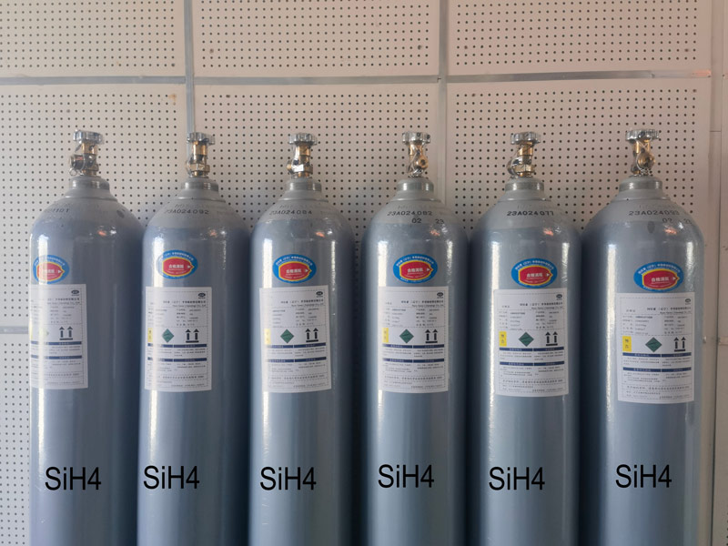
Silane is supplied in compressed gas cylinders ranging from 47 liters to 440 liters in capacity. The cylinders are constructed from specialized materials designed to prevent contamination and ensure safe handling. Given silane’s pyrophoric nature, storage and handling require dedicated gas cabinets with continuous exhaust ventilation, fire suppression systems, and automatic shutoff valves.
8.Safety Considerations: Managing the Pyrophoric Nature of Silane
Silane’s pyrophoric nature—its tendency to ignite spontaneously upon exposure to air—demands rigorous safety protocols. Since its introduction to semiconductor manufacturing, there have been numerous serious accidents involving silane equipment, including fatalities and injuries. These incidents underscore the importance of proper safety systems and procedures.
Key safety measures for silane handling include:
8.1 Storage:
Silane cylinders must be stored in gas cabinets or exhausted enclosures, away from combustible materials, oxidizing substances, and ignition sources. Cylinders should be secured to prevent falling or rolling.
8.2 Personal Protective Equipment:
Operators handling silane should wear appropriate PPE, including fire gloves, Nomex suits or firefighter turnout gear, face shields, earplugs, and safety glasses.
8.3 System Design:
Silane delivery systems must incorporate hardware and software safety interlocks to prevent hazardous conditions. Special purging procedures are required before introducing silane into deposition equipment.
8.4 Emergency Response:
Facilities using silane must have established emergency response procedures, including spill containment, fire suppression, and evacuation protocols.
The investment in safety infrastructure—gas cabinets, purge systems, detection equipment, and training—is substantial but non‑negotiable. Any organization working with silane must view safety not as a cost, but as a fundamental requirement of operations.
9.The Road Ahead: Silane in Next‑Generation Semiconductor Manufacturing
As the semiconductor industry pushes toward ever‑smaller geometries and more complex device architectures, the role of silane continues to evolve. Several trends are shaping the future of silane in semiconductor manufacturing:
9.1 Advanced Node Scaling:
The transition to sub‑5nm nodes places unprecedented demands on film quality and uniformity. Ultra‑high‑purity silane (6N to 7N purity) is essential for these leading‑edge applications.
9.2 3D Device Architectures:
The shift to 3D NAND and 3D logic devices requires conformal deposition over extreme aspect ratios. Silane‑based processes are being optimized to achieve the step coverage and uniformity needed for these demanding structures.
9.3 New Deposition Techniques:
Advanced deposition methods such as hot‑wire CVD (HWCVD), electron‑beam‑excited plasma CVD (EBEP‑CVD), and atomic layer deposition (ALD) are expanding the applications for silane. These techniques offer unique advantages in terms of film quality, deposition rate, or temperature compatibility.
9.4 Integration with Emerging Materials:
Silane is increasingly being used in combination with other precursors to deposit silicon‑based alloy films, such as silicon carbide (SiC) and silicon oxynitride (SiON), for specialized applications.
Silane stands as one of the foundational materials of the semiconductor industry—a simple molecule that enables the complex structures at the heart of modern electronics. From the gate electrodes of microprocessors to the passivation layers of power devices, from the channel layers of display backplanes to the barrier films of advanced memory, silane’s versatility and performance have made it indispensable. For the semiconductor professional who understands the nuances of thin‑film deposition, silane is not merely a chemical precursor—it is the enabler of progress, the material that transforms designs into devices, and the foundation upon which the digital age is built.
Would you like a deeper dive into any specific technical parameters or applications?
As an industry leader focused in Specialty Gases , our goal is to support our customers by keeping them at the forefront of their industries. We’re here to help with any questions you might have so you can transform your ideas into reality, and tackle those big science challenges.
Get free consultant, our experts are ready to serve.
(Follow up our update articles on www.asiaisotopeintl.com or send your comments to tao.hu@asiaisotope.com for further communications)