Octafluorocyclopentene (C5F8) Deep Dive: Optimizing High-Precision Etching for Next-Gen Semiconductors
BY Tao, Published Jan 25, 2026
Introduction: The Art and Science of Process Optimization
In semiconductor manufacturing, understanding a material is only the first step. The true craft lies in optimization—systematically adjusting process parameters to extract maximum performance from a given chemistry. With China Isotope Development Co Ltd‘s own workshop to produce fluoride specialty gases, I’ve come to appreciate that optimization is where laboratory knowledge transforms into manufacturing excellence.
Octafluorocyclopentene (C₅F₈) has emerged as a critical enabler for advanced semiconductor fabrication, offering exceptional selectivity, superior profile control, and significant environmental advantages over legacy fluorocarbon gases. But simply introducing C₅F₈ into a process tool doesn’t guarantee optimal results. Like a precision instrument, C₅F₈ must be carefully tuned—its plasma parameters adjusted, its gas mixtures engineered, its interactions understood—to deliver the extraordinary performance that next-generation devices demand.
This deep dive explores the nuances of C₅F₈ process optimization. We’ll examine plasma chemistry fundamentals, dissect key process variables, explore gas mixture strategies, and discuss application-specific tuning approaches. Whether you’re a process engineer implementing C₅F₈ for the first time or a veteran seeking incremental improvements, my goal is to provide actionable insights drawn from years of hands-on experience and extensive industry collaboration.
Understanding C₅F₈ Plasma Chemistry: The Foundation of Optimization
Effective optimization begins with fundamental understanding. When Octafluorocyclopentene enters a plasma discharge, it doesn’t simply become “reactive”—it undergoes complex fragmentation and recombination processes that determine etching behavior. Let me walk you through these mechanisms, as they form the basis for all optimization strategies.
Molecular Structure and Fragmentation Pathways
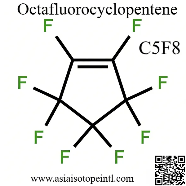
C₅F₈, with its five-membered carbon ring, carbon-carbon double bond, and eight fluorine atoms, presents a unique molecular architecture. The CAS number 559-40-0 identifies this specific compound with molecular weight of 212.04 g/mol. Under plasma conditions, this structure fragments through multiple pathways:
Primary Fragmentation: The carbon-carbon double bond represents the weakest point in the molecule, often breaking first under electron impact. This produces linear C₅Fₓ fragments that subsequently decompose further.
Ring Opening: The cyclic structure can open at various positions, generating a variety of CFₓ species ranging from CF (fluoromethylidyne) to CF₃ (trifluoromethyl radicals).
Fluorine Liberation: Direct fluorine atom abstraction produces atomic fluorine (F*)—the primary etchant species responsible for removing silicon-based materials through volatile SiF₄ formation.
Polymer Precursors: Larger fragments, particularly CF₂ and CF, serve as building blocks for fluorocarbon polymer deposition—the passivation layer that protects sidewalls and mask materials.
The Etch-Deposition Balance
Here’s the critical insight that experienced process engineers understand intuitively: C₅F₈ plasma chemistry represents a dynamic balance between etching (material removal) and deposition (polymer formation). This balance isn’t fixed—it shifts based on plasma parameters, surface conditions, and gas composition.
Fluorine-rich conditions favor etching. More atomic fluorine means faster silicon removal, but potentially at the cost of selectivity as mask materials also experience attack.
Carbon-rich conditions favor deposition. More CFₓ polymer precursors mean thicker sidewall passivation and better mask protection, but potentially slower etch rates and risk of “etch stop” from excessive polymer accumulation.
The optimization challenge is finding the sweet spot—sufficient fluorine for effective etching, sufficient polymer formation for selectivity and profile control, with neither dominating excessively.
Surface-Dependent Reactions
Adding complexity, C₅F₈ plasma chemistry behaves differently on different surfaces:
Silicon surfaces: Ion bombardment prevents polymer accumulation, exposing the surface to fluorine attack. Etching proceeds readily, forming volatile SiF₄ products.
Silicon dioxide surfaces: Similar to silicon, but with additional oxygen released from the oxide contributing to fluorine regeneration through COF₂ formation.
Photoresist surfaces: Lower ion bombardment on vertical sidewalls allows polymer accumulation, forming the protective layer responsible for selectivity.
Chamber walls: Polymer deposition occurs on cool surfaces distant from the plasma, requiring periodic cleaning but also serving as a fluorine “sink” that affects plasma composition.
Understanding these surface-dependent behaviors is essential for predicting how parameter changes will affect overall process performance.
Key Process Parameters: The Optimization Variables
With plasma chemistry fundamentals established, let’s examine the primary variables available for optimization. Each parameter influences the etch-deposition balance differently, and understanding these relationships enables systematic process tuning.
RF Power: Controlling Energy Input
Radio-frequency power drives plasma generation and sustains the reactive species population. In modern etch tools, power is typically applied at two positions:
Source Power (often 13.56 MHz or higher frequencies applied to an upper electrode or coil) controls plasma density—the concentration of ions and radicals. Higher source power means more reactive species, generally increasing etch rates proportionally.
Bias Power (typically lower frequency, applied to the wafer chuck) controls ion energy—how hard ions strike the wafer surface. Higher bias power increases ion bombardment energy, enhancing anisotropy but potentially causing physical damage.
Optimization Strategy: For C₅F₈ processes, I typically recommend starting with moderate source power (sufficient for stable plasma) and incrementally adjusting bias power to achieve desired profile characteristics. Higher bias favors vertical profiles but may compromise selectivity; lower bias improves selectivity but risks tapered profiles.
A practical starting point for 300mm processing: source power of 800-1200W, bias power of 100-300W, then adjusting based on results.
Chamber Pressure: Balancing Reactions
Pressure profoundly influences plasma chemistry by affecting mean free path (the average distance species travel between collisions), residence time (how long molecules remain in the reaction zone), and ion energy distribution.
Lower pressure (5-20 mTorr): Longer mean free path, more directional ion bombardment, enhanced anisotropy. However, lower radical density may reduce etch rates.
Higher pressure (50-100 mTorr): More collisions, higher radical density, faster etch rates. But ion scattering increases, potentially compromising profile verticality.
Optimization Strategy: For high-aspect-ratio features requiring extreme anisotropy, operate at lower pressures (10-30 mTorr). For applications prioritizing throughput where modest aspect ratios are acceptable, higher pressures enable faster processing. C₅F₈ typically performs well across the 15-50 mTorr range, with optimal pressure depending on specific application requirements.
Gas Flow Rate: Controlling Supply and Residence Time
Flow rate determines how much fresh C₅F₈ enters the chamber and how long it remains before being pumped away.
Higher flow rates: Continuous fresh gas supply, more consistent plasma chemistry, but potentially wasteful of expensive specialty gas.
Lower flow rates: Longer residence time allows more complete fragmentation, potentially more efficient utilization, but risks depletion effects and inconsistent chemistry.
Optimization Strategy: I recommend determining minimum flow for stable operation, then operating at 20-30% above this threshold to ensure consistency. Typical C₅F₈ flows range from 5-30 sccm (standard cubic centimeters per minute) depending on chamber volume and pumping capacity. The compound’s boiling point of approximately 27°C means it handles easily as a gas under normal fab conditions.
Temperature: Influencing Surface Reactions
Wafer temperature affects both etch rates (through Arrhenius kinetics) and polymer deposition (through sticking coefficients).
Lower temperatures (below 20°C): Enhanced polymer deposition, improved selectivity, but potentially slower etch rates and risk of excessive passivation.
Higher temperatures (above 60°C): Reduced polymer sticking, faster etch rates, but potentially compromised selectivity and profile control.
Optimization Strategy: For C₅F₈ processes requiring maximum selectivity (gate etching, for example), cooler temperatures (10-30°C) generally perform better. For applications where throughput matters more than ultimate selectivity, warmer temperatures accelerate processing. Modern electrostatic chucks enable precise temperature control, and I recommend systematic temperature studies during process development.
Gas Mixture Engineering: The Power of Combinations
While pure C₅F₈ delivers excellent performance, strategic addition of other gases can fine-tune behavior for specific applications. This “gas mixture engineering” represents one of the most powerful optimization approaches available.
Oxygen Addition: Controlling Polymer Formation
Adding small amounts of O₂ (typically 5-20% of total flow) dramatically affects the etch-deposition balance:
Mechanism: Oxygen reacts with CFₓ polymer precursors, forming volatile CO, CO₂, and COF₂. This reduces polymer deposition rate and liberates additional fluorine for etching.
Effect: Higher etch rates, reduced selectivity to photoresist, thinner sidewall passivation.
Application: When C₅F₈ processes produce excessive polymer (manifesting as “etch stop” or tapered profiles), oxygen addition provides a straightforward solution. Start with 5% O₂ and increase incrementally until desired balance is achieved.
Caution: Excessive oxygen addition can completely suppress passivation, eliminating C₅F₈’s selectivity advantage. Monitor mask erosion carefully when optimizing oxygen content.
Argon Addition: Enhancing Ion Bombardment
Argon, a chemically inert noble gas, participates only through physical mechanisms:
Mechanism: Argon ions provide additional bombardment energy without adding chemical reactivity. They also improve plasma stability and help sputter polymer from horizontal surfaces.
Effect: Enhanced anisotropy, improved polymer clearing from feature bottoms, more stable plasma.
Application: For deep, high-aspect-ratio features where polymer accumulation at trench bottoms limits etch depth, argon addition (10-30% of total flow) improves penetration. The argon ion bombardment clears passivation from horizontal surfaces, allowing etching to proceed.
Nitrogen Addition: Modifying Surface Chemistry
Nitrogen, while relatively inert, does participate in plasma chemistry:
Mechanism: Nitrogen species can incorporate into deposited polymer, modifying its properties. N₂ also dilutes reactive species, moderating etch rates.
Effect: Modified polymer characteristics, potentially more conformal passivation, moderate rate reduction.
Application: Some specialized applications benefit from nitrogen-modified passivation. I’ve seen nitrogen addition improve uniformity across wafers with varying pattern densities by moderating local etch rate variations.
Hydrogen Addition: Scavenging Fluorine
Adding H₂ to C₅F₈ plasmas provides selective fluorine scavenging:
Mechanism: Hydrogen preferentially reacts with fluorine atoms, forming HF and reducing free fluorine concentration. This shifts the balance toward deposition.
Effect: Significantly enhanced selectivity (sometimes exceeding 20:1 silicon-to-photoresist), thicker passivation, reduced etch rates.
Application: For applications demanding ultimate selectivity—extremely thin mask layers, for example—hydrogen addition provides a powerful tuning mechanism. However, HF formation raises safety and chamber compatibility considerations.
Multi-Gas Mixtures: Complex Optimization
Advanced processes often employ three- or four-gas mixtures (for example, C₅F₈/O₂/Ar or C₅F₈/O₂/N₂/Ar) to achieve precise control over multiple process characteristics simultaneously. Optimizing such mixtures requires systematic experimental design approaches—factorial designs, response surface methodology, or machine learning-based optimization—to efficiently navigate the multi-dimensional parameter space.
Application-Specific Optimization Strategies
Different semiconductor applications impose different requirements on etching processes. Let me share optimization strategies for several key applications where C₅F₈ has demonstrated particular value.
Shallow Trench Isolation (STI) Etching
STI creates the isolation structures that prevent electrical interference between adjacent transistors. Requirements include:
- Vertical sidewalls (88-90° from horizontal)
- Smooth surfaces for subsequent oxide filling
- Minimal corner rounding at trench tops
- Precise depth control (typically 200-400nm)
Optimization Approach: Operate at moderate pressure (20-40 mTorr) with bias power sufficient for good anisotropy. Include small argon flow (10-15%) for plasma stability. Temperature around 20-40°C balances selectivity and throughput. Monitor sidewall angle using cross-sectional SEM (scanning electron microscopy) and adjust bias power incrementally until target angle is achieved.
Gate Electrode Etching
Gate etching defines the transistor switching element—perhaps the most critical etch in chip manufacturing. Requirements include:
- Extreme selectivity to thin gate oxides underneath
- Minimal CD loss (target dimension change below 2nm)
- Profile control across varying gate lengths
- Low damage to underlying materials
Optimization Approach: Prioritize selectivity by operating at lower temperatures (10-25°C) and avoiding oxygen addition. Bias power should be minimized consistent with acceptable profile control. Consider hydrogen addition if selectivity remains insufficient. Endpoint detection becomes critical—over-etching even briefly can damage gate oxides.
High-Aspect-Ratio Contact/Via Etching
Creating the vertical connections between metal layers requires etching extremely deep, narrow holes—sometimes with aspect ratios exceeding 50:1. Requirements include:
- Maintaining vertical profile through entire depth
- Avoiding “bowing” (mid-depth widening)
- Preventing etch stop from polymer accumulation
- Clearing all material at feature bottom
Optimization Approach: Lower pressure (15-25 mTorr) maximizes ion directionality. Include argon (20-30%) to assist polymer clearing from feature bottoms. Consider multi-step processes: an initial breakthrough step with higher oxygen to establish the feature, followed by a main etch with optimized selectivity, and a final over-etch with enhanced polymer clearing to ensure complete material removal.
3D NAND Memory Channel Etching
Modern 3D NAND structures require etching through 100+ alternating layers to create channel holes—perhaps the most demanding etch application in semiconductor manufacturing. Requirements include:
- Extreme aspect ratios (approaching 100:1 in latest designs)
- Uniform profile through miles of different materials
- Preventing “twisting” or “tilting” of features
- Maintaining critical dimensions throughout depth
Optimization Approach: This application pushes C₅F₈ to its limits and often requires sophisticated process schemes. Cyclic processes alternating between etch and deposition steps can maintain profile control through extreme depths. Temperature modulation during processing can help manage polymer buildup. Detailed process modeling and simulation become essential for understanding plasma transport into such extreme geometries.
Advanced Optimization Techniques: Beyond Standard Parameters
For engineers seeking ultimate performance, several advanced techniques offer additional optimization dimensions.
Pulsed Plasma Processing
Rather than operating with continuous plasma, pulsed techniques modulate power on millisecond timescales:
Synchronous Pulsing: Source and bias power pulsed together, allowing controlled plasma “on” and “off” periods. During “off” periods, polymer deposition continues without ion bombardment, potentially improving selectivity.
Asynchronous Pulsing: Source and bias power pulsed independently, enabling even finer control. For example, source-on/bias-off periods allow radical generation without ion bombardment.
Benefits for C₅F₈: Pulsed plasmas can enhance selectivity by allowing polymer accumulation during bias-off periods while maintaining anisotropy through directional ion bombardment during bias-on periods.
Temperature Ramping
Rather than maintaining constant temperature, dynamic temperature profiles during etching can optimize different process phases:
Cool Start: Begin at lower temperature for maximum selectivity during initial etching through thin layers.
Warm Finish: Increase temperature during bulk etching phase for improved throughput.
This approach requires sophisticated chuck control but can improve overall process performance beyond what’s achievable with isothermal processing.
Gas Flow Modulation
Similar to pulsed plasma, gas flows can be modulated to create time-varying plasma chemistry:
Cyclic C₅F₈/O₂: Alternating between C₅F₈-only (maximum passivation) and C₅F₈+O₂ (maximum etching) phases can achieve performance impossible with steady-state conditions.
Deposition/Etch Cycling: Deliberate cycles of deposition (C₅F₈-rich conditions) and etching (oxygen-rich conditions) enable precise profile engineering.
In-Situ Monitoring and Feedback Control
Advanced fabs increasingly employ real-time plasma diagnostics:
Optical Emission Spectroscopy (OES): Monitors plasma composition by analyzing light emission from excited species. Can detect process drift or endpoint.
Langmuir Probes: Measure plasma density and electron temperature, providing direct feedback on plasma conditions.
Mass Spectrometry: Samples exhaust gas composition, enabling direct measurement of etch products and unreacted feed gas.
Integrating these diagnostics with feedback control systems enables adaptive optimization—automatically adjusting parameters in response to measured plasma conditions.
Troubleshooting Common Issues: Practical Problem-Solving
Even optimized processes occasionally encounter problems. Here are common issues and their solutions based on my extensive troubleshooting experience.
Problem: Excessive Mask Erosion
Symptoms: Photoresist mask consumption faster than expected, feature CD larger than target.
Likely Causes: Insufficient polymer formation, excessive ion energy, too much oxygen in mixture.
Solutions: Reduce oxygen flow, lower bias power, reduce wafer temperature, consider hydrogen addition for extreme cases.
Problem: Tapered Profiles (Non-Vertical Sidewalls)
Symptoms: Feature wider at top than bottom, sloped sidewalls.
Likely Causes: Excessive polymer deposition on sidewalls, insufficient ion bombardment, pressure too high.
Solutions: Increase bias power, reduce pressure, add small amount of oxygen, increase argon fraction.
Problem: Etch Stop (Incomplete Etching)
Symptoms: Etching halts before reaching target depth, material remaining at feature bottom.
Likely Causes: Excessive polymer accumulation at feature bottom, particularly in high-aspect-ratio features.
Solutions: Increase argon flow to enhance physical sputtering, increase oxygen to reduce polymer formation, use multi-step process with more aggressive clearing step.
Problem: Bowing (Mid-Depth Widening)
Symptoms: Features wider in middle than at top or bottom.
Likely Causes: Ion scattering at feature mid-depth, lateral etching from isotropic radical component.
Solutions: Reduce pressure to minimize scattering, use cyclic etch/deposition process to maintain sidewall protection, ensure consistent temperature control.
Problem: Micro-Trenching (Notches at Feature Bottom)
Symptoms: Small grooves or notches at corners where feature bottom meets sidewall.
Likely Causes: Reflected ion bombardment concentrating at corners, local polymer deficiency.
Solutions: Reduce bias power, increase passivation (lower temperature, reduce oxygen), consider specialized endpoint techniques to avoid over-etching.
The Future of C₅F₈ Optimization: Emerging Frontiers
Looking forward, several developments will shape future C₅F₈ optimization approaches.
Machine Learning-Driven Optimization
The high-dimensional parameter space of modern etch processes—power, pressure, flows, temperature, pulsing parameters, mixture compositions—exceeds human intuitive optimization capability. Machine learning algorithms can efficiently explore these spaces, identifying non-obvious optimal conditions and predicting process outcomes from parameter inputs.
I’m already seeing early adoption of ML-based process control in advanced fabs, and expect this trend to accelerate dramatically.
Atomic-Scale Process Control
As devices push toward true atomic-scale dimensions—gate-all-around transistors with channel thicknesses of a few atomic layers—etching must achieve atomic-layer precision. Atomic Layer Etching (ALE) techniques, which remove exactly one atomic layer per cycle, represent the ultimate precision.
C₅F₈’s controllable polymer chemistry may enable development of ALE processes where alternating C₅F₈ exposure (surface modification) and argon bombardment (removal) cycles achieve self-limiting atomic-layer removal.
Integration with Advanced Patterning
Extreme ultraviolet (EUV) lithography and multi-patterning schemes create new demands on etch processes. Thinner resists, more complex pattern geometries, and tighter overlay requirements all influence optimal C₅F₈ process conditions.
Close collaboration between lithography and etch teams becomes essential—optimization isn’t just adjusting etch parameters, but co-optimizing the entire patterning sequence.

Conclusion: The Ongoing Journey of Optimization
Octafluorocyclopentene (C₅F₈) represents a remarkable tool for semiconductor manufacturing—offering the selectivity, profile control, and environmental benefits that next-generation devices demand. But realizing its full potential requires thoughtful, systematic optimization tailored to specific applications and continuously refined as requirements evolve.
The optimization principles outlined in this deep dive—understanding plasma chemistry fundamentals, systematically exploring key parameters, engineering gas mixtures for specific objectives, and applying advanced techniques for ultimate performance—provide a framework for extracting maximum value from C₅F₈ processes.
After decades in this field, I remain fascinated by the depth of understanding required to truly master a process chemistry. Each application presents unique challenges; each fab has different equipment characteristics; each technology node pushes previous limits. Optimization is never “complete”—it’s an ongoing journey of learning, experimentation, and refinement.
For process engineers embarking on C₅F₈ implementation or seeking to improve existing processes, I encourage systematic approaches, careful documentation, and willingness to challenge conventional assumptions. The rewards—improved yields, better device performance, reduced environmental impact—justify the investment in optimization excellence.
The semiconductor industry’s continued advancement depends on our collective ability to push process technologies beyond current boundaries. C₅F₈ optimization represents one critical frontier in this ongoing quest. Hopefully these insights contribute to your success in mastering this powerful chemistry for next-generation semiconductor manufacturing.
Would you like a deeper dive into any specific technical parameters or applications?
As an industry leader focused in Specialty Gases products, our goal is to support our customers by keeping them at the forefront of their industries. We’re here to help with any questions you might have so you can transform your ideas into reality, and tackle those big science challenges.
Get free consultant, our experts are ready to serve.
(Follow up our update articles on www.asiaisotopeintl.com or send your comments to tao.hu@asiaisotope.com for further communications)