From Graphene to SiC: Methane‑Based CVD Solutions Driving the Future of Power Electronics and 5G Devices
BY Tao, Published Jan 27, 2026
1. Introduction: Why Methane‑Based CVD Matters Now
Power electronics and 5G radio‑frequency (RF) systems are moving into a new era defined by higher voltages, higher switching frequencies and far stricter efficiency targets. Electric vehicles, fast DC chargers, smart grids and massive‑MIMO 5G base stations all demand devices that can handle more power, more heat and more bandwidth in ever smaller volumes.
This is why wide‑bandgap (WBG) semiconductors such as silicon carbide (SiC), and two‑dimensional (2D) materials such as graphene, have moved from research labs into mainstream roadmaps. Both material classes are now strongly linked by one enabling technology:
Methane‑based chemical vapor deposition (CVD).
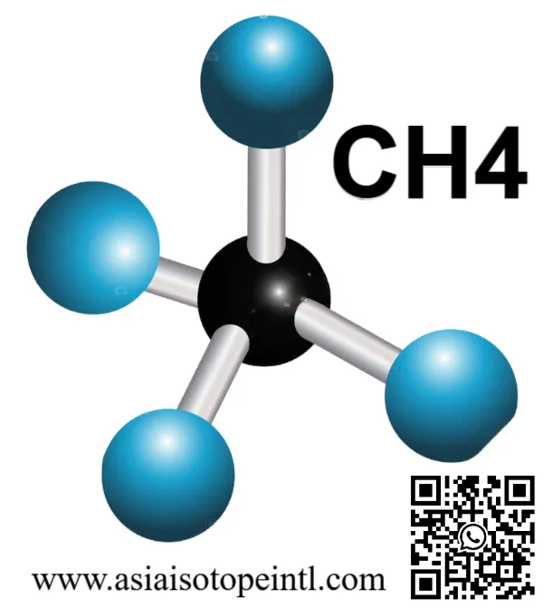
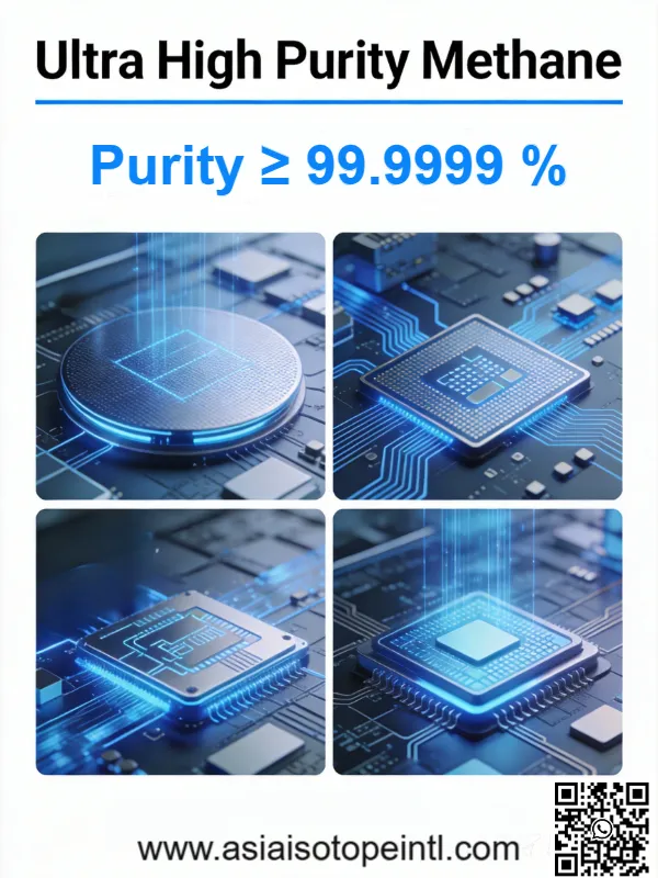
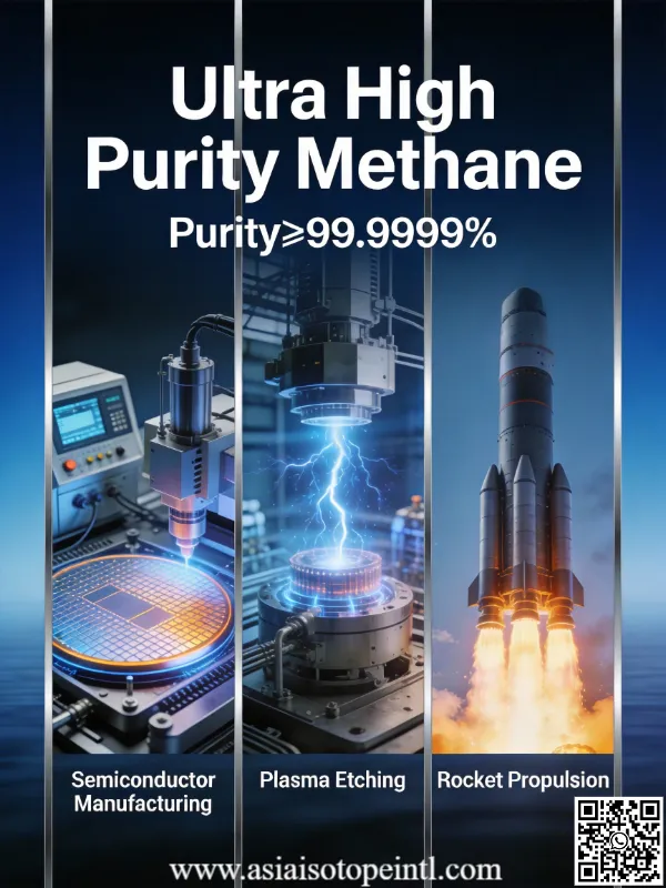
Methane (CH₄) is far more than a simple hydrocarbon fuel in this context. In advanced semiconductor manufacturing, ultra‑high‑purity methane is a precision carbon source. It enables:
- Large‑area, uniform graphene for RF, sensing and thermal applications
- High‑quality SiC epitaxial layers for next‑generation power MOSFETs and diodes
- Tunable interfaces and doping profiles in compound semiconductors for 5G RF front ends
As China Isotope Development Co Ltd was starting to supply Ultra High Purity Methane (UHP CH4) to China domestic clients, I see methane‑based CVD as one of the most strategically important building blocks for the next decade of electronics. This article will look at the topic from lab to fab: from the fundamentals of methane chemistry, through graphene and SiC growth, to practical considerations like gas purity, safety and supply‑chain robustness.
2. The Role of Methane in CVD: A “Clean” Carbon Lever
2.1 Why Methane and Not “Any” Hydrocarbon?
In CVD, we bring precursor gases to a hot surface so they decompose and deposit a solid film. For carbon‑containing materials, we have many choices—methane, ethylene, acetylene, propane and various organometallic precursors.
Methane is often preferred because it is:
- Chemically simple – One carbon, four hydrogens. Fewer decomposition pathways mean more controllable film chemistry.
- Relatively stable at lower temperatures – It does not react prematurely in the gas phase, which reduces particle formation and keeps the reactor and wafer surfaces cleaner.
- Capable of clean decomposition at elevated temperature – Above ~900–1000 °C on catalytic surfaces (like copper or nickel), methane cracks into active carbon species that can build ordered structures such as graphene or crystalline SiC.
- Well understood and easy to purify – The industrial gas industry has decades of experience delivering methane at extremely low impurity levels (down to parts‑per‑billion or lower for O₂, H₂O and other contaminants).
For graphene and SiC alike, control over the carbon supply is fundamental. Too much carbon, or carbon released at the wrong moment, causes unwanted nucleation, polycrystalline films, surface roughening or defect generation. Methane’s relatively “gentle” behavior under typical CVD conditions makes it a precise tuning knob for process engineers.
2.2 Purity: Carbon Source as an Electrical Performance Limiter
In power electronics and RF devices, electrical performance is extremely sensitive to deep‑level defects and unintentional doping. Trace oxygen, moisture, sulfur, or metallic species can introduce:
- Higher leakage currents
- Lower breakdown voltages
- Reduced carrier mobility and lifetime
- Device‑to‑device variability and poor yield
Because methane is often fed into high‑temperature, highly reactive environments, any impurity it carries is likely to end up either in the film or at a critical interface. This is why device‑grade methane is not just “99.999% pure” in a generic sense; it is very carefully engineered and analyzed for specific contaminants that are known to degrade WBG semiconductors.
In short: the carbon source is part of the device design, not just a commodity gas.
3. Methane‑Based CVD for Graphene: From Copper Foils to RF Substrates
3.1 Fundamentals of Graphene CVD on Metals
The most widely adopted route to large‑area graphene uses low‑pressure CVD (LPCVD) with methane as the carbon source and copper as the catalyst substrate.
A simplified process flow:
- Substrate preparation – High‑purity copper foil or film is annealed (often in hydrogen) to increase grain size and smooth the surface.
- Growth stage – Methane diluted in hydrogen is introduced at ~900–1050 °C under reduced pressure. Copper catalyzes the decomposition of methane into active carbon.
- Nucleation and growth – Carbon atoms diffuse on the copper surface, nucleate, and grow laterally to form graphene domains.
- Coalescence – Domains merge into a continuous monolayer (or bilayer/few‑layer depending on conditions).
- Cooling and transfer – The graphene film is often transferred onto a functional substrate (SiO₂/Si, quartz, polymers, etc.) for device fabrication.
The methane flow rate, partial pressure and growth time are the main tuning knobs for:
- Domain size and density
- Number of layers (mono‑ vs multi‑layer graphene)
- Defect density (grain boundaries, vacancies)
- Uniformity over large areas (up to 8‑ or 12‑inch wafers in advanced lines)
Too high a methane concentration can lead to dense nucleation and multilayer growth. Too low, and growth may be incomplete or non‑uniform. The key is to reach a regime where the copper surface is just supersaturated enough with carbon to maintain lateral growth without triggering thickening.
3.2 Gas‑Phase and Surface Chemistry: Why Methane Quality Shows Up in Raman Spectra
The quality of CVD graphene is routinely evaluated using Raman spectroscopy (D, G and 2D peaks), electrical measurements (sheet resistance, carrier mobility) and microscopy.
Impurities in methane or the carrier gas can manifest as:
- Enhanced D‑peak intensity (more defects and disorder)
- Higher sheet resistance and lower mobility
- Increased unintentional doping (p‑ or n‑type behavior due to adsorbed species or substitutional impurities)
Typical culprits include:
- Oxygen and water – They oxidize the copper surface, disturb nucleation kinetics and introduce oxygenated defects in the graphene lattice.
- Hydrocarbon “heavies” – Heavier hydrocarbons can crack at different temperatures, causing inhomogeneous deposition and multilayer “islands”.
- Sulfur‑ or halogen‑containing species – Can etch, dope or introduce complex point defects in graphene.
From a gas engineering standpoint, an optimized graphene CVD line uses:
- Ultra‑high‑purity methane with tight specs on O₂, H₂O, total hydrocarbons and sulfur
- Hydrogen carrier gas with similarly tight impurity control
- Point‑of‑use purifiers and online analyzers to detect contamination events in real time
This is where specialized gas suppliers bring real value: not only providing gas, but ensuring the entire gas path (cylinder → gas cabinet → VMB/VMP → tool) is consistent with sub‑ppm or even sub‑ppb impurity targets.
3.3 Graphene’s Relevance for 5G and Beyond
Why does this matter to 5G and future wireless systems?
Graphene offers a unique set of properties that complement traditional semiconductors:
- Ultra‑high carrier mobility – Potentially supporting very high‑frequency analog and RF operation.
- Excellent thermal conductivity – Useful as an in‑package heat spreader for hot RF power amplifiers.
- Mechanical flexibility and transparency – Enabling flexible antennas and transparent conductive films.
In the near term, methane‑grown graphene is particularly relevant for:
- RF passives and interconnects – Low‑loss, tunable RF structures on glass, sapphire or flexible substrates.
- On‑chip thermal management – Graphene heat spreaders integrated with Si, SiC or GaN power devices.
- EMI shielding and antennas – Lightweight, conformal solutions for 5G mmWave modules.
All of these applications rely on wafer‑scale, uniform graphene films that only methane‑based CVD can practically deliver today. The transfer from copper to the target substrate remains a challenge, but direct growth on dielectrics, metals and even SiC is advancing rapidly, again with methane as the controllable carbon source.
4. Methane‑Based CVD for SiC: The Backbone of Modern Power Electronics
If graphene is the “glamorous” 2D material, silicon carbide is the workhorse of real‑world power electronics. From 650 V devices for onboard chargers to multi‑kilovolt modules for grid converters, SiC is enabling:
- Lower switching losses vs silicon
- Higher junction temperatures
- More compact, efficient power conversion systems
4.1 Epitaxial SiC Growth: Where Methane Comes In
SiC power devices (MOSFETs, Schottky diodes, IGBTs under development) are built on epitaxial layers grown on SiC substrates. These layers are produced in CVD reactors using:
- A silicon precursor (commonly silane, SiH₄, or chlorinated silanes)
- A carbon precursor (methane, CH₄, or sometimes propane, C₃H₈)
- A carrier gas, typically high‑purity hydrogen
At temperatures around 1500–1650 °C and reduced pressure, these precursors react near the hot substrate surface to form a crystalline SiC layer with a specified:
- Polytype (commonly 4H‑SiC for power electronics)
- Thickness (from a few micrometers to >100 µm for some high‑voltage devices)
- Doping concentration (n‑type or p‑type, often in the 10¹⁵–10¹⁷ cm⁻³ range)
The Si:C ratio, total gas flow, and temperature profile are tightly controlled. Here, methane’s chemical behavior is a key lever:
- It decomposes in a controlled manner, helping to avoid gas‑phase nucleation (“soot” or particles).
- Its relatively low sticking coefficient helps maintain step‑flow growth—a growth mode where the crystal grows smoothly along atomic steps rather than forming new 3D islands.
- It can support high growth rates while maintaining low defect densities with proper reactor design.
Many high‑volume production lines have standardized on methane‑based recipes because they offer a good balance between growth rate, morphology, and device‑grade crystal quality.
4.2 Defect Engineering: Carbon Source as a Quality Gate
In SiC epitaxy, defects such as:
- Micropipes
- Basal plane dislocations (BPDs)
- Stacking faults
- Carrot and triangular defects
have direct impact on device breakdown voltage, on‑resistance and long‑term reliability. While the substrate quality is critical, the epitaxial process can:
- Propagate or annihilate existing defects
- Introduce new defects via thermal stress, contamination or stoichiometry imbalances
The carbon precursor gas influences:
- Vacancy concentrations – Carbon‑rich vs silicon‑rich conditions shift the balance between Si and C vacancies in the crystal lattice.
- Surface roughness and step bunching – Oversupply of carbon can lead to rough, faceted surfaces that degrade MOS channel mobility and increase electric‑field hot spots.
- Incorporation of unintentional impurities – Any hetero‑atom impurity in the methane (e.g., oxygen, sulfur, metals) can enter the SiC lattice or remain at extended defects, acting as recombination centers or trap states.
For high‑voltage SiC devices (3.3 kV, 6.5 kV and beyond), the epitaxial layer may be tens of micrometers thick. Over such thicknesses, even extremely low impurity levels in methane can accumulate to concentrations that matter. That is why device manufacturers are specifying:
- Methane purity not only in “N‑number” terms (e.g., 6N, 7N) but in customized impurity matrices tailored to SiC needs.
- Consistent batch‑to‑batch and cylinder‑to‑cylinder performance, backed by analytical data and statistical process control on the gas supplier side.
4.3 SiC in Power Electronics and 5G Infrastructure
SiC epi grown with methane‑based CVD is already present in:
- EV powertrains – Inverters, onboard chargers and DC‑DC converters.
- Fast DC chargers – Higher efficiency, smaller footprints and reduced cooling requirements.
- Industrial drives and renewable energy inverters – Improved efficiency in wind and solar installations.
- 5G base station power supplies – Highly efficient, compact switch‑mode power supplies and DC‑DC converters feeding RF PAs and digital logic.
In other words, while the public discussion around 5G often focuses on RF front‑ends and antennas, the power conversion backbone of these systems is increasingly built on SiC. And that backbone is as good as the epitaxy—and therefore the methane supply—that underpins it.
5. Linking Graphene and SiC: Complementary Roles in 5G and Next‑Gen Electronics
5.1 Graphene on SiC and Hybrid Stacks
There is a fascinating convergence where graphene and SiC are not just parallel stories, but actually intersect.
One example is epitaxial graphene on SiC, where graphene is formed by the controlled sublimation of silicon from the surface of a SiC wafer at very high temperatures, leaving behind a carbon‑rich interface that forms graphene. Even when methane is not the direct source of carbon in this specific process, methane‑based epitaxy is often used to engineer the underlying SiC layers and interfaces beforehand.
In more advanced integration schemes, we can envision:
- Graphene heat spreaders directly deposited—or transferred—onto SiC power dies to improve thermal management.
- Graphene interconnects and RF passives on SiC or GaN‑on‑SiC RF front‑ends, offering low‑loss, tunable and potentially flexible elements.
In these hybrid stacks, the methane‑based CVD processes for both materials must be carefully harmonized so that impurity profiles, thermal budgets and surface chemistries are all compatible.
5.2 GaN‑on‑SiC RF PAs: Indirect but Crucial Roles for Methane
Many state‑of‑the‑art 5G power amplifiers for base stations use GaN‑on‑SiC structures: a GaN (gallium nitride) epitaxial stack grown on semi‑insulating SiC substrates. While the growth of GaN itself is typically done by MOCVD (metal‑organic CVD) using organometallic Ga precursors and ammonia, the SiC substrate and buffer structures are often the product of earlier methane‑based processes (epitaxy and/or wafer finishing).
Thus, methane indirectly supports:
- Higher power density RF devices (GaN‑on‑SiC vs GaN‑on‑Si)
- Better thermal performance (thanks to SiC’s high thermal conductivity)
- Smaller, more efficient RF front‑end modules in base stations and potentially in user equipment over time
For both power electronics and RF systems, the methane supply chain becomes strategically important: device manufacturers need long‑term assurance that gas quality, specifications and availability can keep pace with aggressive capacity expansions in SiC and related materials.
6. Engineering the Gas: From Ultra‑High Purity to Isotopic Methane
6.1 Beyond “Pure”: Tailored Methane Specifications
From a specialty gas engineering perspective, providing methane for advanced CVD is much more than filling cylinders.
A robust offering typically covers:
- Custom impurity limits – For example, specifying oxygen, moisture, total sulfur, halides and selected metals at levels well below generic “electronic grade” specs.
- Lot traceability and analytical certificates – Every cylinder or batch is accompanied by detailed analysis, enabling fabs to correlate process excursions with gas data if needed.
- Distribution system engineering – Design of gas cabinets, valves, purifiers and distribution manifolds to minimize dead volumes and adsorption/desorption behavior that can cause “memory effects” for reactive impurities.
- Real‑time monitoring – Integration of oxygen, moisture and sometimes hydrocarbon analyzers into the gas lines to give early warning of leaks, purifier exhaustion or regulator issues.
This is especially important in multi‑reactor, high‑throughput environments, where an impurity spike that persists for even a few hours can scrap large numbers of wafers.
6.2 Isotopically Engineered Methane: A Frontier for Advanced Devices
Although still a niche, isotopically enriched methane (for example, ¹²CH₄ or ¹³CH₄ with high isotopic purity) is emerging as a tool for advanced material engineering:
- In graphene and other 2D materials, isotopic composition can influence phonon scattering and therefore thermal conductivity.
- In diamond CVD (another methane‑based process closely related to SiC and graphene growth), isotopic purity has a major impact on spin coherence times for quantum devices.
These are early‑stage but exciting directions where gas isotopic composition becomes a design parameter, not just a background detail. For suppliers deeply involved in isotope gases and methane purification, this represents a high‑value, high‑differentiation niche aligned with the most advanced electronic and quantum technologies.
7. CVD Reactor and Process Considerations for Methane‑Based Growth
7.1 Hot‑Wall vs Cold‑Wall, Horizontal vs Vertical
CVD reactors for graphene and SiC vary widely in configuration, but some common themes apply:
- Hot‑wall reactors (often used for SiC epitaxy) provide uniform temperature distribution but require careful material selection to avoid graphite or SiC coating spalling.
- Cold‑wall or showerhead reactors (more common in some graphene and compound semiconductor applications) localize the heat near the wafer, reducing undesired deposition on walls.
For methane‑based CVD, reactor design must balance:
- Gas‑phase vs surface reactions – We want methane to decompose predominantly at or near the wafer surface, not in the bulk gas where it forms particles.
- Residence time and flow patterns – Sufficient time for reaction, but not so long that gas‑phase nucleation dominates.
- Scalability – From single‑wafer R&D reactors to multi‑wafer, high‑throughput production tools.
Changing methane concentration, total flow, or carrier gas composition often requires re‑optimizing flow dynamics and temperature uniformity. This is why process transfer from one tool family to another is non‑trivial, even if the “recipe” looks similar on paper.
7.2 Process Windows and Metrology
Defining a stable “process window” for methane‑based CVD typically involves:
- Temperature – For graphene: ~900–1050 °C; for SiC epi: ~1500–1650 °C.
- Pressure – From a few Torr (LPCVD) up to atmospheric pressure for some configurations.
- Gas ratios – CH₄/H₂ for graphene; CH₄/SiH₄/H₂ for SiC, often with additional dopant precursors (e.g., nitrogen or aluminum sources).
Metrology plays a crucial role:
- For graphene: Raman mapping, sheet resistance mapping, Hall measurements, AFM and optical inspection.
- For SiC: X‑ray diffraction (XRD), optical microscopy, defect inspection tools, capacitance‑voltage (C–V) profiling and lifetime measurements.
Because many of the critical outcomes (like deep‑level defects or interface trap densities) are sensitive to subtle changes in impurity levels, feedback between fab metrology and gas supply analytics becomes increasingly important as processes mature.
8. Environmental and Safety Aspects of Methane‑Based CVD
8.1 Safety: Flammability and Explosion Risk
Methane is a flammable gas with a wide explosive range in air. Safe operation in semiconductor fabs requires:
- Certified gas cabinets with automatic shutoff valves, gas detectors and fire suppression systems.
- Proper ventilation and exhaust design, including dedicated exhaust lines for flammable gases.
- Rigorous leak‑check and maintenance procedures on all fittings, valves and regulators.
Modern gas handling systems are designed so that, under normal operating conditions, personnel are never directly exposed to methane flow, and any leak is quickly detected and contained.
8.2 Environmental Considerations
Methane is also a potent greenhouse gas. Although semiconductor fabs consume only a tiny fraction of global methane compared to energy or agriculture, responsible companies increasingly:
- Optimize CVD recipes and utilization efficiency to minimize gas usage per wafer.
- Implement abatement systems (oxidizers, combustors or plasma abatement) to break down unreacted methane and reaction by‑products before exhaust is released.
- Monitor and report greenhouse gas emissions as part of broader ESG (environmental, social and governance) policies.
Interestingly, when methane is fully oxidized to CO₂ and water in an abatement system, the overall greenhouse impact per molecule of carbon is reduced compared to venting methane directly. Thus, proper abatement is not only a safety measure but also a climate responsibility.
9. Strategic Outlook: Methane‑Based CVD in the Era of Power Electronics, 5G and Beyond
Looking forward over the next 5–10 years, several trends make methane‑based CVD even more central to advanced electronics:
- Scaling of SiC production
- Rapid expansion of SiC wafer and epi capacity for EVs, renewables and industrial drives.
- Tighter performance specifications on breakdown voltage, on‑resistance and reliability—driving stricter demands on methane purity and consistency.
- Integration of 2D materials with WBG semiconductors
- Graphene and related 2D materials moving from discrete R&D demonstrations towards integration with Si, SiC and GaN platforms.
- New device concepts (heterostructure transistors, high‑performance interconnects, advanced RF passives) that rely on high‑quality, methane‑grown graphene.
- 5G evolution and paving the way to 6G
- Higher frequencies (mmWave and beyond) and more compact, integrated antenna‑in‑package solutions where materials like graphene or SiC‑based substrates can shine.
- Increasing need for efficient, high‑power RF PAs and ultra‑compact power supplies—both areas where SiC, and therefore methane‑based epitaxy, play a central role.
- Materials innovation enabled by isotopic and chemical tailoring of methane
- Fine control over carbon isotopes and impurity profiles enabling new quantum, RF and thermal management functionalities.
- Potential crossover into ultra‑wide‑bandgap materials such as diamond and related carbides, where methane CVD is already a cornerstone.
Throughout this landscape, specialty gas expertise—from raw methane production and purification, through isotopic selection, to fab‑level distribution engineering—will be a decisive differentiator. Device manufacturers will increasingly partner with gas specialists who understand not just how to deliver a cylinder, but how tiny variations in gas quality map directly onto wafer‑level metrics and ultimately system‑level performance.
10. Conclusion
From copper‑catalyzed graphene sheets for RF and thermal management, to thick, defect‑controlled SiC epitaxy for high‑voltage power devices, methane‑based CVD has become one of the core enablers of modern and future electronics.
What appears at first glance to be a simple carbon‑bearing gas is, in reality, a finely tunable process parameter:
- Its decomposition kinetics govern film nucleation, growth mode and morphology.
- Its impurity profile directly affects defect densities, carrier lifetime, and breakdown behavior.
- Its isotopic and chemical customization opens doors to new material functionalities in 2D materials, WBG and ultra‑WBG systems.
As power electronics proliferate in EVs, fast charging and grid infrastructure, and as 5G (and future 6G) architectures demand ever more efficient and compact RF and power solutions, the quiet role of methane in CVD reactors becomes strategically important.
Investing in:
- Robust methane purification and analytical capabilities
- Carefully engineered delivery and monitoring systems
- Close collaboration between process engineers, device designers and gas suppliers
will pay off in higher yields, better performance and faster time‑to‑market for the next generation of power and RF devices.
In that sense, the journey “from graphene to SiC” is more than a catchy phrase; it is a roadmap that runs straight through the heart of methane‑based CVD solutions—and the specialty gas expertise behind them.
Would you like a deeper dive into any specific technical parameters or applications?
As an industry leader focused in Specialty Gases products, our goal is to support our customers by keeping them at the forefront of their industries. We’re here to help with any questions you might have so you can transform your ideas into reality, and tackle those big science challenges.
Get free consultant, our experts are ready to serve.
(Follow up our update articles on www.asiaisotopeintl.com or send your comments to tao.hu@asiaisotope.com for further communications)