Electronic Grade Methane (CH4) in SiC Epitaxy: Unlocking High-Voltage, High-Temperature Third-Generation Semiconductors
BY Tao, Published Jan 18, 2026
Introduction: The Carbon Key to Powering Tomorrow’s Electronics
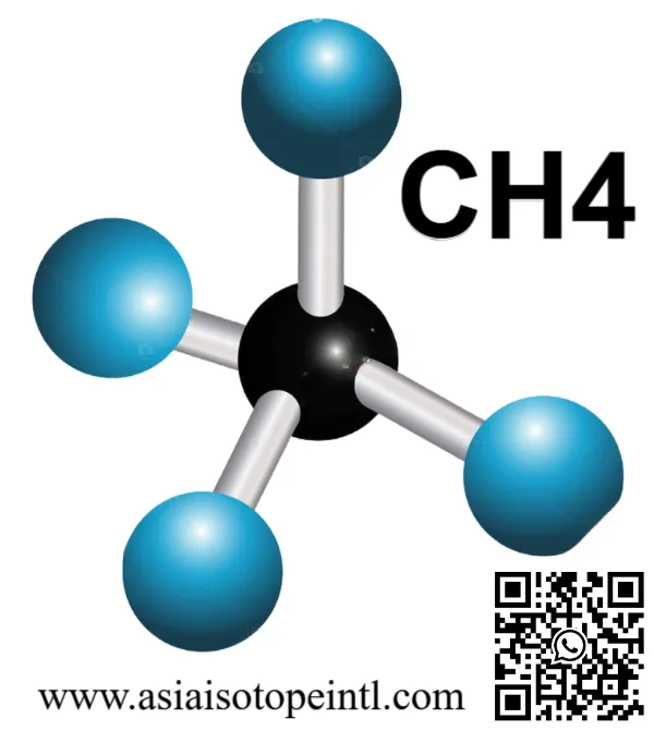
In the intricate world of specialty gases, where molecules are scrutinized down to parts-per-billion impurities, few gases are as deceptively simple yet profoundly impactful as methane (CH4). As China Isotope Development Co Ltd was starting to supply Ultra High Purity Methane (UHP CH4) to China domestic clients, I’ve witnessed firsthand how the right gas purity can make or break billion-dollar wafer runs. Today, electronic grade methane is emerging as a pivotal enabler in silicon carbide (SiC) epitaxy—the precise art of growing crystalline layers for third-generation semiconductors.
Third-generation semiconductors like SiC and gallium nitride (GaN) are supplanting traditional silicon in high-stakes applications: electric vehicles (EVs), renewable energy inverters, and aerospace power systems. Why? SiC handles voltages up to 10 kV and temperatures exceeding 600°C, where silicon melts or fails. These “wide-bandgap” materials promise 10x efficiency gains, slashing energy losses in everything from EV chargers to grid-scale solar farms.
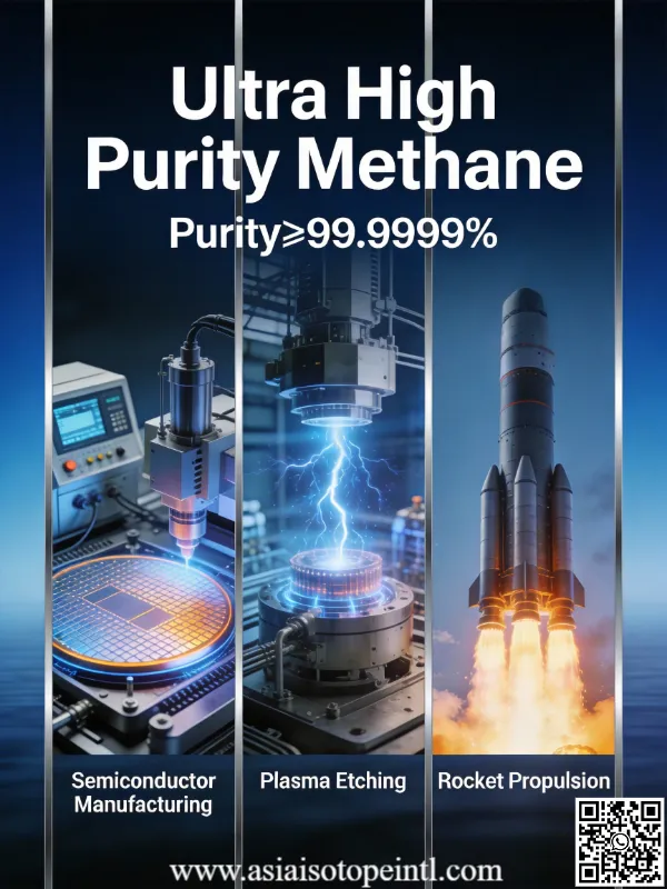
At the heart of SiC device manufacturing lies epitaxial growth via chemical vapor deposition (CVD), where methane serves as the carbon precursor. But not just any methane—electronic grade CH4, with purity levels of 99.999% (5N) or higher and moisture below 1 ppm, is non-negotiable. Impurities introduce defects that cascade into device failures, costing fabs millions.
1. The Dawn of Third-Generation Semiconductors: Why SiC is the Future
Semiconductors have evolved in generations: first (Si), second (GaAs), and now third (SiC, GaN). Silicon, our workhorse for decades, hits limits at 150-200°C and ~1 kV breakdown voltage. Enter SiC: a crystalline compound of silicon and carbon with a 3.26 eV bandgap—three times silicon’s—enabling operation at 600°C+ and electric fields 10x stronger.
Key Properties Driving Adoption
- High Breakdown Voltage: SiC MOSFETs (metal-oxide-semiconductor field-effect transistors) support 1,200V to 20kV ratings, ideal for EV traction inverters where silicon IGBTs (insulated-gate bipolar transistors) waste 5-10% energy as heat.
- Thermal Management: Thermal conductivity of ~490 W/m·K dissipates heat efficiently, shrinking cooling systems by 50%.
- Switching Speed: Faster electron mobility reduces losses in high-frequency apps like 5G base stations and AI data centers.
Market projections underscore the shift: SiC power devices are forecast to hit $11B by 2030, fueled by EVs (projected 40M units/year by 2030) and renewables. Wolfspeed’s 300mm SiC breakthrough in 2026 signals scalability for AI and AR/VR power needs.
Yet, SiC’s promise hinges on flawless epitaxial layers. Substrates (4H-SiC polytype, most common) are cut from boules, then epi-grown with doped layers 5-100μm thick. Defects like basal plane dislocations (BPDs) or micropipes kill yield. Here, precursor gases are king—and methane is ascending the throne.
2. SiC Epitaxy Fundamentals: Building Atom-by-Atom Perfection
Epitaxy (“epi” = upon, “taxy” = order) grows single-crystal films on a substrate, mirroring its lattice. For SiC, horizontal hot-wall CVD reactors operate at 1,400-1,800°C, 50-200 mbar, using hydrogen carrier gas.
The CVD Process Step-by-Step
- Precursors Introduced: Silicon source (silane SiH4 or dichlorosilane DCS) + carbon source (propane C3H8 or methane CH4).
- Pyrolysis: At high T, precursors decompose: SiH4 → Si + 4H; CH4 → C + 2H2 (simplified).
- Surface Reactions: Si and C atoms adsorb, migrate, and bond in the substrate’s lattice, forming SiC.
- Growth Rate: Typically 5-20 μm/hr, controlled by C/Si ratio (0.8-1.2).
The reaction is site-competition epitaxy: Steps on the substrate (from off-axis polishing, 4-8°) nucleate growth, propagating laterally to bury defects.
Chloride-based CVD (using HCl or chlorinated silanes) enhances growth rates to 100 μm/hr for high-voltage epi, but carbon source choice dictates quality.
3. Methane as the Carbon Precursor: From Skepticism to Superiority
Historically, propane dominated SiC epi due to easier decomposition and higher carbon yield. Early studies deemed methane unsuitable, citing low reactivity at SiC growth temps (needs >1,600°C for efficient cracking).
But innovation flipped the script. Recent chloride-based CVD shows methane excels:
- Smoother Morphology: Methane yields pit-free surfaces vs. propane’s triangular defects at high C/Si ratios.
- Longer Carrier Lifetime: Minority carrier lifetime >10 μs with CH4 vs. propane, critical for power devices.
- Flexible C/Si Window: Methane allows precise tuning (wider range), optimizing thick growth (125μm demos).
In my gas lab, we’ve analyzed effluents: Methane pyrolysis leaves fewer heavy residues, reducing homogeneous nucleation (gas-phase particles contaminating wafers).
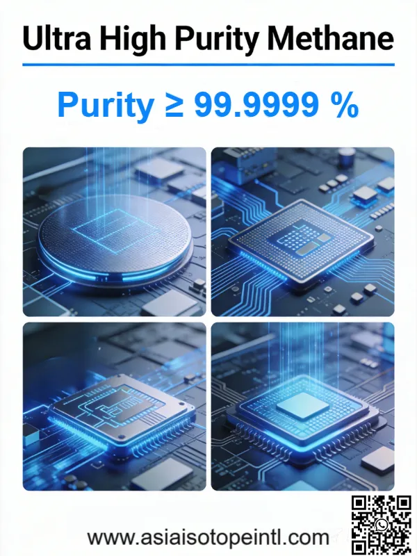
4. The Imperative of Electronic Grade Purity in CH4
Purity isn’t optional—it’s existential. Electronic grade CH4 specs:
| Impurity | Max Level (ppb or ppm) |
|---|---|
| H2O | ≤1 ppmv |
| O2 | ≤10 ppb |
| N2 | ≤50 ppb |
| Total Hydrocarbons | ≤100 ppb (excl. CH4) |
| Assay | ≥99.999% (5N) |
Moisture hydrolyzes to OH radicals, etching SiC or doping unintentionally. Oxygen forms SiO2 inclusions, scattering carriers. Nitrogen introduces shallow donors, shifting resistivity.
In practice, 99.9% methane spikes defect densities 10x; 6N (99.9999%) enables <1 BPD/cm² epi. Production involves cryogenic distillation, catalytic purification (O2/H2O getters), and GC-MS verification—processes I oversee routinely.
5. Optimizing Growth: C/Si Ratios, Doping, and Defect Control
Growth rate μ = k * [C/Si]^n * P_total^m, where k is kinetic constant.
Methane enables C/Si=1.0±0.1 without morphology degradation, vs. propane’s narrower window.
Doping Precision
- Nitrogen (N2 or NH3): N-type, 10^14-10^18 cm⁻³ for drift layers.
- Aluminum (TMA): P-type.
Methane’s clean decomposition minimizes carbon vacancies (V_C), stabilizing doping uniformity <5%.
Defect mitigation: High-purity CH4 reduces triangle pits (from Si droplets) by 50%, per recent studies.
Ultra High Purity Methane UHP CH4
6. Breakthroughs in Thick Epitaxial Layers for High-Voltage Devices
High-voltage SiC (6.5kV-20kV) demands 50-120μm epi. Traditional propane struggles >50μm with stress/cracks.
Methane shines: 125μm layers at 20μm/hr, low doping (10^14 cm⁻³), breakdown >10kV. Recent H2/CH4 ratio tweaks yield nanowires or bulk-like growth.
7. Real-World Applications: EVs, Renewables, and Beyond
- EVs: SiC inverters cut losses 2/3, extending range 10%. Tesla, Porsche adopt.
- Renewables: Solar/wind inverters at 1.7kV handle grid spikes.
- Industrial/Aerospace: High-temp motors, rail traction.
- Emerging: AI PSUs, 300mm SiC for datacenters.
By 2026, SiC EVs save 1B tons CO2 annually.
Conclusion: Methane‘s Monumental Role in SiC Supremacy
Electronic grade methane isn’t just a precursor—it’s the precision tool unlocking SiC’s potential. Its purity quells defects, flexibility optimizes growth, and advantages over propane propel high-voltage epi. As third-gen semis electrify the world, methane will fuel efficiency revolutions, from EVs to exascale computing.
From my vantage in gas field, the message is clear: Invest in purity, harvest power.
Would you like a deeper dive into any specific technical parameters or applications?
As an industry leader focused in Specialty Gases products, our goal is to support our customers by keeping them at the forefront of their industries. We’re here to help with any questions you might have so you can transform your ideas into reality, and tackle those big science challenges.
Get free consultant, our experts are ready to serve.
(Follow up our update articles on www.asiaisotopeintl.com or send your comments to tao.hu@asiaisotope.com for further communications)