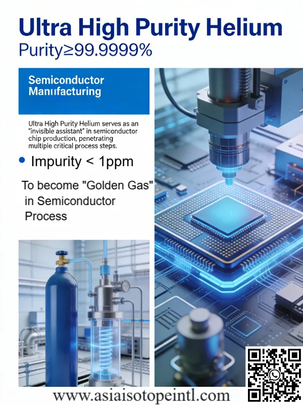
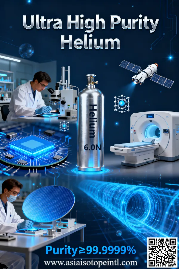
Ultra High Purity Helium 99.9999%: Essential CVD Process Gas for Next-Gen Semiconductor Manufacturing
BY Tao, Published Jan 11, 2026
In the intricate, almost microscopic world of semiconductor manufacturing, the difference between a revolutionary microchip and a piece of useless silicon often comes down to the invisible. We often marvel at the complex lithography machines or the architectural genius of a 2-nanometer node, but as someone who has spent decades analyzing the fluid dynamics and chemical properties of electronic specialty gases, I can tell you that the true heroes are often the gases that permeate these systems.
Among these, Helium is the “Noble King.” But not just any helium. We are talking about Ultra High Purity (UHP) Helium, specifically the 99.9999% (6N) grade.
As we transition into the era of Angstrom-level manufacturing, where “Next-Gen” implies architectures like Gate-All-Around (GAA) transistors and 3D stacking, the purity requirements for process gases have shifted from “stringent” to “absolute.” Today, I want to take a deep dive into why 6N Helium is not just a commodity, but a critical engineering component in Chemical Vapor Deposition (CVD), the process that builds the very foundations of modern electronics.

1. Defining “6N”: The Physics of 99.9999% Purity
To understand the value, we must first quantify the standard. In the industrial gas world, we use the “N” nomenclature.
- 4N (99.99%): Standard balloon or welding grade.
- 5N (99.999%): The baseline for laboratory chromatography.
- 6N (99.9999%): The semiconductor standard.
The difference between 5N and 6N might seem mathematically trivial—a mere 0.0009% difference. However, in the realm of semiconductor physics, we measure impurities in parts per million (ppm) and parts per billion (ppb).
5N Helium allows for a total impurity content of 10 ppm (parts per million). 6N Helium mandates a total impurity content of 1 ppm or less.
Why does this 9 ppm gap matter?
Imagine a swimming pool filled with perfectly clear water. If you drop a single cup of dye into it, the water changes color slightly. In a 5N scenario, you have ten cups of “contaminants”—oxygen, moisture (H2O), nitrogen, hydrocarbons—floating in your process chamber.
In a CVD process creating a dielectric film that is only a few atoms thick, a single molecule of water acts like a boulder on a highway. It causes nucleation sites, creates pinholes, disrupts the crystal lattice, and alters the electrical resistivity of the layer. When you are manufacturing logic chips with billions of transistors, a 10 ppm impurity level is catastrophic for yield rates. 6N purity ensures that the “noise” in the chemical reaction is effectively silenced.
2. The Role of Helium in Chemical Vapor Deposition (CVD)
Chemical Vapor Deposition (CVD) is the process of depositing thin films of solid material onto a silicon wafer by exposing it to volatile precursors, which react and/or decompose on the wafer surface.
While Helium is inert—meaning it doesn’t chemically react to become part of the film itself—it is the ideal Carrier Gas and Diluent. Here is the expert breakdown of why UHP Helium is irreplaceable in this role.
A. The Master of Thermal Conductivity
One of the most unique properties of helium is its thermal conductivity. It conducts heat better than any other gas except hydrogen. However, hydrogen is highly reactive and flammable, making it unsuitable for many oxidizing CVD steps.
In a CVD reactor, maintaining a precise, uniform temperature across the wafer is paramount. A temperature variance of just 0.5°C can lead to uneven film thickness.
- UHP Helium acts as a thermal bridge. When mixed with precursor gases, it ensures that thermal energy is distributed rapidly and evenly.
- Backside Cooling: In many CVD and etching chucks, 6N Helium is pumped behind the wafer to transfer heat away from the substrate, preventing the wafer from warping under the intense heat of the reaction. If this helium contains moisture (low purity), it creates steam, oxidizing the backside of the wafer and contaminating the vacuum chamber.
B. High Diffusivity and Uniformity
Helium atoms are incredibly small and light. This gives helium high diffusivity. When transporting heavy, complex precursor molecules (like TEOS for oxide deposition or metal-organics for interconnects) into the reaction chamber, you need a carrier gas that can move quickly and spread out evenly.
- Heavier gases like Argon can create “dead zones” or laminar flow issues where the concentration of the precursor is higher in the center of the wafer than the edges.
- UHP Helium, due to its low density, promotes a more uniform distribution of the reactant gas mixture. This ensures that the deposited film has consistent thickness and stoichiometry from the center of the wafer to the very edge—critical for maximizing the number of usable chips per wafer.
C. Plasma Stability in PECVD
In Plasma Enhanced Chemical Vapor Deposition (PECVD), we use an electric field to turn the gas into plasma, allowing deposition at lower temperatures. Helium has the highest ionization potential of all elements (24.59 eV). This might sound counterintuitive—isn’t hard-to-ionize bad? Actually, in a mix, helium acts as a buffer. It stores energy in its “metastable” states. When a metastable helium atom collides with a precursor molecule, it transfers that energy efficiently (Penning ionization), helping to break down the precursor controllably without creating an overly aggressive plasma arc that could damage the delicate wafer surface. 6N purity is vital here: If impurities like Nitrogen are present, they ionize much easier than Helium, stealing the energy and destabilizing the plasma, leading to defects.
3. The Impurity Threat: What Happens When You Don’t Use 6N?
Let’s look at the specific damage caused by common impurities found in lower-grade helium during the CVD process.
Oxygen (O2)
- The Effect: Unwanted Oxidation.
- The Result: If you are depositing a pure metal layer (like Tungsten or Cobalt) for interconnects, oxygen impurities will oxidize the metal, increasing its electrical resistance. This causes “RC Delay”—slowing down the speed at which signals move through the chip. In the logic sector, speed is everything.
Moisture (H2O)
- The Effect: The “Killer” Defect.
- The Result: Water is the hardest impurity to remove from a vacuum system. In CVD, water molecules can get trapped inside the dielectric layers. Later, during high-temperature annealing, this trapped water expands or reacts, causing the film to crack or delaminate (peel off). Furthermore, moisture reacts with precursor gases (like Chlorine-based precursors) to form acids, corroding the gas delivery lines and the chamber itself.
Hydrocarbons (CnHm)
- The Effect: Carbon Contamination.
- The Result: Carbon creates “leakage paths” in insulating layers. If a transistor is supposed to be “off,” carbon impurities might allow a tiny current to leak through, draining the battery life of the final device (like a smartphone) and generating excess heat.
Using 99.9999% Helium eliminates these variables. It provides the process engineer with a “blank canvas,” ensuring that the only chemistry happening in the chamber is the chemistry they intended.
4. Next-Gen Applications: Beyond Standard CVD
As we look toward the future of the semiconductor industry, specifically node sizes below 5nm, the role of UHP Helium expands into even more critical territories.
Atomic Layer Deposition (ALD)
ALD is the successor to CVD for ultra-thin films. It builds layers one atomic row at a time. The process relies on sequential pulses of precursors and purge gases.
- Between every chemical pulse, the chamber must be purged completely of the previous chemical.
- UHP Helium is the preferred purge gas because its small atomic size allows it to sweep through high-aspect-ratio structures (deep, narrow trenches in the chip) and flush out residual chemicals faster than Nitrogen or Argon.
- If the purge gas isn’t 6N pure, it introduces contaminants precisely at the interface between atomic layers, destroying the device’s quantum properties.
3D NAND and High-Aspect Ratio Etching
Modern memory chips (3D NAND) are built like skyscrapers, with over 200 layers stacked vertically. Etching vertical holes through these layers requires high-energy plasma.
- UHP Helium is used to cool the wafer during this intense bombardment.
- It is also mixed into the plasma to control the “profile” of the hole, ensuring it goes straight down and doesn’t bow outwards.
EUV Lithography
While not CVD, the Extreme Ultraviolet (EUV) lithography process that defines the patterns for CVD requires a vacuum environment. However, some cooling and purging flows are necessary.
- EUV light is absorbed by almost everything. Only Hydrogen and Helium are transparent enough to be allowed anywhere near the optical path.
- 6N Helium is used to protect the precious mirrors and reticles in these $150 million machines from contamination.
5. The Supply Chain and Quality Assurance of UHP Helium
Producing 6N Helium is an engineering marvel in itself. Helium is typically extracted from natural gas deposits where it has been trapped for millions of years.
The Purification Gauntlet
To reach 99.9999%, crude helium undergoes:
- Cryogenic Distillation: Cooling the gas to near absolute zero. Since Helium has the lowest boiling point of any element (-269°C), everything else (Nitrogen, Methane, Argon) turns to solid or liquid and drops out.
- Pressure Swing Adsorption (PSA): Using specialized carbon molecular sieves to trap trace impurities.
- Getter Purification: For the final cleaning, the gas is passed over heated metal alloys (getters) that chemically bond with the final few parts per billion of Oxygen or Nitrogen.
The “Last Mile” Challenge: Cylinders and Distribution
You can produce 6N gas, but can you deliver it? A standard steel cylinder has rough walls that can trap moisture. For 6N Helium, we use specially treated cylinders (often internally polished and vacuum-baked) with ultra-high integrity diaphragm valves.
- Leak Integrity: A microscopic leak in a valve doesn’t just let helium out; it lets the atmosphere in due to partial pressure differences, instantly downgrading the gas from 6N to 4N.
- Quality Analysis: Verifying 6N purity requires sophisticated equipment like Atmospheric Pressure Ionization Mass Spectrometry (APIMS), capable of detecting impurities at the ppt (parts per trillion) level.
6. Conclusion: The Invisible Backbone of the Digital Age
In the grand scheme of the “Energy Revolution” and the “Digital Transformation,” we often focus on the macro—the solar panels, the wind turbines, the data centers. But as a specialist, I urge you to look at the micro.
The progression of Moore’s Law is slowing down. We are hitting the physical limits of silicon. To squeeze more performance out of chips, we are relying on materials engineering and atomic-level precision. In this regime, Ultra High Purity Helium (99.9999%) is not merely a utility. It is a process enabler.
- It protects the integrity of the crystal lattice.
- It enables the thermal management of nanoscale reactions.
- It allows for the precise deposition of layers only a few atoms thick.
Without 6N Helium, the yield of 3nm and 2nm chips would collapse. The cost of electronics would skyrocket, and the pace of innovation would stall.
Companies like China Isotope Development Co.,Ltd, who are rooting themselves deeply in the purification and supply of this “Golden Gas,” are essentially the custodians of the semiconductor roadmap. By mastering the technology to produce and maintain 6N purity, they ensure that the global semiconductor industry has the pristine environment it needs to build the future.
Whether for Semiconductors, Aerospace, Quantum Computing, or MRI Healthcare, the demand for purity is non-negotiable. As we push the boundaries of science, our tools must be sharper, and our materials must be purer. UHP Helium is the standard-bearer for this new age of precision.
Would you like a deeper dive into any specific technical parameters or applications?
As an industry leader focused in Specialty Gases products, our goal is to support our customers by keeping them at the forefront of their industries. We’re here to help with any questions you might have so you can transform your ideas into reality, and tackle those big science challenges.
Get free consultant, our experts are ready to serve.
(Follow up our update articles on www.asiaisotopeintl.com or send your comments to tao.hu@asiaisotope.com for further communications)