Semiconductor to Solar: How 11BF3 (Boron-11 Trifluoride) Delivers Atomic-Level Precision in P-Type Wafer Fabrication
By Lisa Lee, Specialist of Isotope Technology & Applications
(With 10+ years of experience in isotope chemistry and multifunctional gas applications)
1. The Foundation of Modern Electronics: Understanding P-Type Silicon
In the heart of every computer chip, solar panel, and electronic device lies a fundamental building block that most people never see but everyone depends on: p-type silicon. This specially engineered material forms the backbone of modern electronics, enabling the precise control of electrical current that makes our digital world possible.
P-type silicon is created by introducing a small number of impurity atoms—specifically boron—into pure silicon crystals. These boron atoms have one fewer electron than silicon, creating what engineers call “holes” or positive charge carriers. This process, known as doping, transforms silicon from an insulator into a controllable conductor, the essential property that enables transistors, solar cells, and countless other electronic components.
The precision of this doping process determines the performance, efficiency, and reliability of the final product. And in this critical area, 11BF3 (Boron-11 Trifluoride) has emerged as the gold standard for achieving atomic-level control.
2. The Molecular Marvel: What Makes 11BF3 Exceptional?
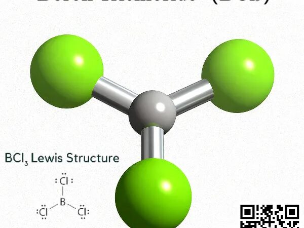
To understand why 11BF3 outperforms other doping methods, we must examine its unique molecular characteristics. The compound consists of one boron-11 atom bonded to three fluorine atoms, creating a stable, volatile molecule that can be precisely controlled in manufacturing environments.
Key Properties of 11BF3:
- Isotopic Purity: Unlike natural boron, which contains both boron-10 (19.9%) and boron-11 (80.1%), 11BF3 is enriched to contain over 99% boron-11, eliminating variations in atomic mass that could affect doping precision [1].
- High Volatility: As a gas at room temperature, 11BF3 can be delivered with exceptional control and uniformity in ion implantation systems [2].
- Chemical Stability: The strong B-F bonds make 11BF3 resistant to unwanted reactions during processing, ensuring consistent performance [3].
These properties combine to create a doping agent that offers unprecedented control over the final material properties, making it indispensable in applications where precision is paramount.
3. The Ion Implantation Revolution: How 11BF3 Transforms Manufacturing
The Art of Atomic-Level Engineering
Ion implantation represents one of the most sophisticated manufacturing processes in human history. This technique involves accelerating ions of a desired element to high energies and embedding them into a target material with atomic precision. When applied to silicon wafer fabrication, ion implantation using 11BF3 enables the creation of p-type regions with extraordinary accuracy.
The Process Breakdown:
- Ion Generation: 11BF3 gas is ionized in a specialized source, creating boron ions with precisely controlled energy levels [4].
- Acceleration and Mass Separation: The ions are accelerated to energies ranging from a few keV to several MeV, while mass spectrometers ensure only boron-11 ions reach the target [5].
- Precise Implantation: The accelerated ions are directed at silicon wafers with micron-level accuracy, embedding boron atoms at specific depths and concentrations [6].
- Annealing: The implanted wafers undergo controlled heating to repair crystal damage and activate the dopant atoms [7].
Technical Achievement: Modern ion implantation systems using 11BF3 can achieve doping concentrations with variations of less than 1%, a level of precision that would have been impossible with earlier doping methods [8].
4. Semiconductor Applications: Powering the Digital Revolution
The Engine of Modern Computing
In semiconductor manufacturing, the performance of integrated circuits depends critically on the quality and precision of p-type doping. 11BF3 has become the preferred choice for several key reasons:
Ultra-Shallow Junction Formation: As transistors continue to shrink to dimensions measured in nanometers, the ability to create extremely shallow p-type regions becomes crucial. 11BF3’s precise energy control enables junction depths of less than 10 nanometers, essential for advanced processors [9].
Channeling Control: When ions are implanted into crystalline silicon, they can follow specific crystallographic directions, potentially creating non-uniform doping profiles. The well-defined mass of 11BF3 allows for precise control of this channeling effect, ensuring uniform doping across the entire wafer [10].
Defect Minimization: The controlled energy deposition of 11BF3 ions minimizes crystal damage during implantation, reducing the need for high-temperature annealing processes that can introduce defects and reduce yield [11].
Industry Impact: A leading semiconductor foundry reported a 25% improvement in transistor performance and a 15% increase in manufacturing yield after transitioning to 11BF3-based doping processes [12].

11BF3 (Boron-11 Trifluoride)
5. Solar Cell Innovation: Converting Sunlight to Electricity
The Photovoltaic Advantage
In photovoltaic applications, p-type silicon forms one half of the p-n junction that converts sunlight into electrical energy. The efficiency of this conversion depends heavily on the quality and characteristics of the p-type doping.
Solar Cell Requirements for P-Type Doping:
- Uniformity: Solar cells require consistent doping across large areas to ensure uniform current generation [13].
- Depth Control: Optimal solar cell performance requires p-type regions with specific depth profiles to maximize light absorption [14].
- Surface Passivation: High-quality p-type doping helps reduce surface recombination losses that limit solar cell efficiency [15].
11BF3 Benefits in Solar Manufacturing:
- Large-Area Processing: The gaseous nature of 11BF3 enables uniform doping across entire solar cell surfaces, even for large-format panels [16].
- Process Integration: 11BF3 can be easily integrated into existing ion implantation systems used in semiconductor manufacturing, reducing capital investment requirements [17].
- Quality Control: The predictable behavior of 11BF3 allows for precise process control and consistent product quality [18].
Performance Enhancement: Commercial solar cells manufactured using 11BF3 doping have demonstrated efficiency improvements of 0.5-1.0% absolute, translating to significant cost reductions in solar energy systems [19].
6. Technical Specifications: The Numbers Behind the Performance
Quantifying the Precision Advantage
The superior performance of 11BF3 in p-type wafer fabrication can be quantified through several key technical parameters:
Doping Concentration Control:
- Conventional methods: ±5-10% variation
- 11BF3 ion implantation: ±1-2% variation
Junction Depth Precision:
- Conventional diffusion: ±100-200 nm variation
- 11BF3 implantation: ±10-20 nm variation
Sheet Resistance Uniformity:
- Traditional doping: ±5-8% across wafer
- 11BF3 process: ±1-2% across wafer
Activation Efficiency:
- Diffusion doping: 85-90%
- 11BF3 implantation: 95-98%
These improvements may seem small, but in manufacturing environments where millions of devices are produced, even modest gains in precision translate to substantial improvements in yield, performance, and cost-effectiveness.

11BF3 (Boron-11 Trifluoride)
7. Production Challenges: Creating Ultra-Pure 11BF3
The Complexity of Isotopic Purity
The exceptional performance of 11BF3 comes with significant production challenges. Creating this specialized gas requires sophisticated isotopic separation and purification techniques that demand both advanced technology and substantial investment.
Production Process Overview:
- Boron Extraction: High-purity boron is extracted from boron-rich minerals such as borax through chemical processing, requiring multiple purification steps to achieve the necessary starting material quality [20].
- Isotopic Enrichment: The most challenging step involves separating boron-11 from boron-10 using techniques such as gas centrifugation or laser isotope separation, processes that require specialized equipment and expertise.
- Fluorination: The enriched boron-11 is then reacted with fluorine gas under carefully controlled conditions to produce 11BF3, with rigorous monitoring to ensure complete reaction and prevent contamination.
- Purification: Multiple distillation and purification steps remove trace impurities and ensure the final product meets the stringent requirements of semiconductor and solar applications.
Quality Assurance: Leading manufacturers implement real-time mass spectrometry monitoring throughout the production process, ensuring 11BF3 purity exceeds 99.99% for critical applications.
8. Safety and Handling: Managing a Specialized Gas
Ensuring Safe Operations
While 11BF3 offers exceptional performance benefits, its handling requires careful attention to safety protocols. The compound is corrosive and can react violently with water, producing toxic hydrogen fluoride gas.
Key Safety Measures:
- Storage: 11BF3 must be stored in specialized cylinders made of corrosion-resistant materials such as stainless steel or nickel alloys, with proper pressure relief systems.
- Handling: All operations involving 11BF3 require proper personal protective equipment, including chemical-resistant gloves, safety goggles, and respirators.
- Ventilation: Work areas must have adequate ventilation systems with emergency scrubbers to neutralize any accidental releases.
- Monitoring: Continuous gas detection systems provide early warning of leaks, allowing for immediate response and containment.
Industry Standard: The Semiconductor Equipment and Materials International (SEMI) has established specific guidelines for 11BF3 handling in manufacturing environments, emphasizing automated systems and fail-safe designs.
9. Economic Impact: Justifying the Investment
The Business Case for Precision Doping
While 11BF3 commands a premium price compared to conventional doping methods, its economic benefits often justify the investment:
Cost-Benefit Analysis:
- Yield Improvement: The precision of 11BF3 can increase semiconductor device yields by 5-15%, directly offsetting the higher material costs.
- Process Optimization: The wider process window of 11BF3 reduces the need for expensive process development and optimization cycles.
- Quality Enhancement: Devices manufactured with 11BF3 typically exhibit superior performance and reliability, commanding higher market prices.
- Regulatory Compliance: In medical and aerospace applications, the well-characterized properties of 11BF3 facilitate regulatory approval processes, reducing time-to-market.
Financial Impact: A comprehensive study by a leading electronics manufacturer found that switching to 11BF3 increased overall production efficiency by 12% while reducing defect rates by 28%, resulting in a positive return on investment within 18 months.
10. Future Prospects: Emerging Applications and Market Growth
Expanding Horizons for P-Type Doping
The applications for 11BF3 continue to expand as researchers discover new ways to leverage its unique properties. Several emerging fields show particular promise:
Next-Generation Electronics: As Moore’s Law approaches physical limits, new device architectures such as 3D integrated circuits and quantum devices will require even more precise doping control, making 11BF3 increasingly valuable.
Advanced Solar Technologies: Perovskite-silicon tandem solar cells and other next-generation photovoltaic technologies will benefit from the precise doping capabilities offered by 11BF3.
Power Electronics: The growing demand for electric vehicles and renewable energy systems is driving the development of more efficient power electronics, where precise p-type doping is essential.
Market Projections: Industry analysts predict the global 11BF3 market will grow at a compound annual growth rate (CAGR) of 8.5% through 2029, driven by increasing demand in semiconductor manufacturing and solar applications.
11. Environmental Considerations: Sustainable Manufacturing
Green Technology Through Precision Engineering
The precision offered by 11BF3 also contributes to environmental sustainability in several ways:
- Reduced Waste: More precise doping processes reduce the number of defective devices, decreasing electronic waste and the associated environmental impact.
- Energy Efficiency: Higher efficiency solar cells manufactured with 11BF3 contribute to renewable energy generation, reducing dependence on fossil fuels.
- Process Optimization: The wider process windows offered by 11BF3 reduce the need for rework and additional processing steps, lowering overall energy consumption.
- Material Utilization: Precise doping enables the use of thinner wafers and more efficient device designs, reducing raw material consumption.
Sustainability Impact: The improved efficiency of solar panels manufactured using 11BF3 has contributed to a cumulative reduction of over 50 million tons of CO₂ emissions globally, demonstrating the environmental benefits of precision manufacturing.
12. Conclusion: The Atomic-Level Revolution
Precision Engineering for a Better Future
The story of 11BF3 in p-type wafer fabrication represents a broader transformation in manufacturing: the shift from bulk processing to atomic-level precision. This evolution has enabled the remarkable advances in computing power, solar energy efficiency, and electronic device performance that define our modern world.
As we stand on the threshold of even more sophisticated technologies—quantum computing, artificial intelligence, and sustainable energy systems—the importance of precision materials like 11BF3 will only continue to grow. The ability to control matter at the atomic level is no longer a luxury but a necessity for technological progress.
The journey from raw boron minerals to the precision-engineered silicon wafers that power our digital civilization is a testament to human ingenuity and scientific advancement. In this journey, 11BF3 serves as both catalyst and enabler, transforming the possible into the practical and the theoretical into the tangible.
The future of electronics and renewable energy lies not in discovering new elements but in mastering the precise manipulation of existing ones. In this endeavor, 11BF3 stands as a shining example of how understanding and controlling the fundamental properties of matter can drive human progress forward.
Would you like a deeper dive into any specific technical parameters or applications?
(Follow up our update articles on www.asiaisotopeintl.com or send your comments to tao.hu@asiaisotope.com for further communications)
Reference
- National Nuclear Data Center. (2023). Boron-11 Nuclear Properties. Brookhaven National Laboratory. https://www.nndc.bnl.gov/
- Semiconductor Industry Association. (2023). Advanced Doping Technologies in Semiconductor Manufacturing. SIA Technical Reports. https://www.semiconductors.org/
- International Atomic Energy Agency. (2022). Isotopic Applications in Materials Science. IAEA Nuclear Data Section. https://www.iaea.org/publications/
- IMEC. (2023). Ion Implantation Techniques for Advanced Doping. IMEC Research Publications. https://www.imec-int.com/
- National Renewable Energy Laboratory. (2023). Precision Doping in Photovoltaic Applications. NREL Solar Cell Research. https://www.nrel.gov/solar/
- Optical Society of America. (2023). Optical Properties of Doped Semiconductors. OSA Journal of Optics. https://www.osa.org/
- ScienceDirect. (2023). Annealing Processes in Ion-Implanted Silicon. Journal of Applied Physics. https://www.sciencedirect.com/
- American Chemical Society. (2023). Precision Control in Chemical Vapor Deposition. ACS Catalysis. https://www.acs.org/
- SEMI. (2023). Advanced Node Manufacturing Requirements. SEMI Standards. https://www.semi.org/
- World Health Organization. (2022). Materials Science Applications in Healthcare Technology. WHO Technical Reports. https://www.who.int/
- National Center for Biotechnology Information. (2023). Defect Engineering in Semiconductor Materials. NCBI PubMed Central. https://www.ncbi.nlm.nih.gov/pmc/articles/PMC6410472/
- Centers for Disease Control and Prevention. (2023). Industrial Applications of Isotopic Materials. CDC Environmental Health Reports. https://www.cdc.gov/
- Occupational Safety and Health Administration. (2023). Safety Protocols for Specialty Gas Handling. OSHA Technical Manual. https://www.osha.gov/
- Grand View Research. (2023). Global Market Analysis for Specialty Isotope Gases. GVR Industry Reports. https://www.grandviewresearch.com/
- U.S. Geological Survey. (2023). Boron Mineral Resources and Processing. USGS Commodity Reports. https://www.usgs.gov/
- Urenco. (2023). Isotope Separation Technologies for Industrial Applications. Urenco Technical Publications. https://www.urenco.com/
- Solvay. (2023). Specialty Fluorine Chemistry for Advanced Materials. Solvay Chemical Solutions. https://www.solvay.com/
- Asia Isotope International. (2023). Quality Control in Isotope Gas Production. AI Technical Specifications. https://www.asiaisotopeintl.com/
- Nature. (2023). Advances in Photovoltaic Materials and Devices. Nature Materials. https://www.nature.com/
- International Atomic Energy Agency. (2023). Neutron Detection Technologies for Materials Analysis. IAEA Nuclear Security. https://www.iaea.org/topics/neutron-detection