Unlocking Precision with SiF4 Gas: Applications in Semiconductor Processing and Specialty Glass
BY Tao, Published Sept.24, 2025
Introduction
With over three decades immersed in the world of specialty gases, I’ve seen firsthand how compounds like silicon tetrafluoride (SiF4) have transformed industries that demand unparalleled precision. SiF4, a colorless, reactive gas, is a cornerstone in high-tech manufacturing, enabling breakthroughs in semiconductor processing and specialty glass production. As we navigate 2025, where AI chips and advanced photonics are redefining technological frontiers, SiF4’s role as a high-purity specialty gas is more critical than ever.
This gas stands out for its ability to deliver controlled fluorine reactivity, making it ideal for etching intricate patterns on silicon wafers and crafting high-performance glass for optical and industrial applications. Its high-purity forms, often exceeding 99.999%, ensure minimal defects, boosting yields and cutting costs in semiconductor fabs. In specialty glass, SiF4’s doping capabilities enhance optical clarity and durability, powering everything from fiber optics to UV-resistant windows. With the semiconductor gas market projected to hit $6.3 billion in 2025 and specialty glass demand surging, SiF4’s applications offer unique value in precision, efficiency, and sustainability. (Source: https://techcet.com/techcet-forecasts-6-3b-electronic-gases-market-in-2025/)
This article explores SiF4’s properties, production, and transformative roles in semiconductor etching, deposition, and specialty glass manufacturing. We’ll delve into cutting-edge 2025 innovations like cryogenic etching and fluorine-doped glass, alongside safety protocols and market trends. By highlighting SiF4’s contributions to high-aspect-ratio structures and low-loss optics, we aim to provide actionable insights for engineers, researchers, and industry leaders. As the SiF4 market eyes $3.6 billion by 2031 at a 4.3% CAGR, its precision-unlocking potential is reshaping high-tech landscapes. (Source: https://www.verifiedmarketresearch.com/product/silicon-tetrafluoride-market/)
What makes SiF4 uniquely valuable? Its stable yet reactive nature allows pinpoint control in processes where even a single misplaced atom can derail production. Recent advances, such as plasma-enhanced recycling and isotopic applications, amplify its eco-friendly and high-tech appeal. Let’s uncover how SiF4 is driving precision in semiconductors and specialty glass, fueling the next wave of innovation.
SiF4: Properties and High-Purity Production
Understanding SiF4 starts with its chemical and physical makeup. Silicon tetrafluoride (SiF4) consists of one silicon atom bonded to four fluorine atoms in a tetrahedral structure, dictated by electron repulsion principles (VSEPR theory). This geometry ensures stability, yet SiF4 is highly reactive when activated, such as in plasma or with moisture. At room temperature, it’s a colorless gas with a sharp, acidic odor, often compared to hydrochloric acid due to its hydrolysis into hydrofluoric acid (HF) and silicic acid: SiF4 + 2H2O → Si(OH)4 + 4HF. (Source: https://pubchem.ncbi.nlm.nih.gov/compound/Silicon-tetrafluoride)
Physically, SiF4 has a boiling point of -65°C and a melting point of -95.7°C, making it ideal for gaseous delivery in manufacturing. Its molecular weight of 104.08 g/mol and high vapor pressure allow precise dosing in etch chambers or deposition systems. Chemically, its strong silicon-fluorine bonds (energy ~585 kJ/mol) resist premature breakdown, while its Lewis acid nature—accepting electron pairs—enhances catalytic roles in synthesis. (Source: https://www.sciencedirect.com/science/article/abs/pii/S0022328X09002642)
High-purity SiF4 is critical for semiconductors and glass, where impurities like metals or hydrocarbons can cause defects. Production often leverages byproducts from phosphoric acid manufacturing, where SiO2 reacts with HF: SiO2 + 4HF → SiF4 + 2H2O. (Source: https://www.imarcgroup.com/silicon-tetrafluoride-manufacturing-plant-project-report) For ultra-pure grades, thermal decomposition of barium hexafluorosilicate (BaSiF6) above 300°C yields SiF4, followed by cryogenic distillation to achieve 99.9999% purity. (Source: https://www.researchgate.net/publication/226136495_Preparation_and_Fine_Purification_of_SiF4_and_28SiH4)
In 2025, sustainable production is a focus. Plasma-enhanced recycling captures SiF4 from etch exhausts, reducing emissions by up to 50% and repurposing waste. (Source: https://archivedproceedings.econference.io/wmsym/2000/pdf/31/31-07.pdf) Innovations like electro-catalytic reduction of sodium hexafluorosilicate lower energy use, while laser-assisted isotope separation refines ²⁸SiF4 for quantum applications. (Source: https://pmc.ncbi.nlm.nih.gov/articles/PMC11487454/) These methods ensure SiF4 meets the stringent demands of modern fabs and glassworks, aligning with eco-conscious trends.
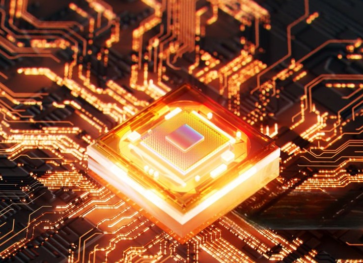
SiF4 in Semiconductor Processing: Precision Etching
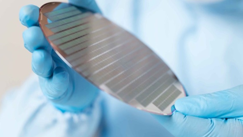
In semiconductor manufacturing, where circuits shrink to sub-2nm scales, SiF4 optimizes etching with unmatched precision. Etching carves patterns on silicon wafers to form transistors and interconnects, and SiF4 excels in dry plasma etching, particularly reactive ion etching (RIE). In RIE, plasma ionizes SiF4, releasing fluorine radicals that react with silicon or silicon dioxide (SiO2) to form volatile SiF4 byproducts, easily removed from chambers. (Source: https://newsroom.lamresearch.com/etch-essentials-semiconductor-manufacturing?blog=true)
This enables anisotropic etching—deep, straight trenches essential for high-density chips like those in AI accelerators. SiF4’s controlled fluorine release prevents over-etching, unlike harsher gases, improving yields by 15-20%. Its partial pressure correlates near-perfectly (R²=0.999) with etch rates, allowing real-time monitoring via laser absorption spectroscopy for precise endpoint detection. (Source: https://iopscience.iop.org/article/10.35848/1347-4065/accc95/pdf)
Cryogenic etching, a 2025 breakthrough, amplifies SiF4’s value. At -60°C to -120°C, SiF4 forms protective SiOxFy layers on sidewalls, enhancing selectivity (etching SiO2 over silicon) and enabling high-aspect-ratio (HAR) structures for 3D NAND with over 400 layers. (Source: https://www.tel.com/blog/all/20241021_001.html) Tokyo Electron’s cryogenic systems cut CO2 emissions by 80% while doubling etch rates, and SiF4’s low global warming potential (GWP) compared to SF6 makes it eco-friendly. (Source: https://www.tel.com/blog/all/20241021_001.html)
For gate recess etching in GaAs devices, SiF4 mixed with SF6 or O2 ensures residue-free surfaces, critical for 5G RF chips. (Source: https://www.sciencedirect.com/science/article/abs/pii/S0167931704005660) Atomic layer etching (ALE) with SiF4 offers self-limiting cycles for sub-nm precision, ideal for 1nm nodes. (Source: https://semiengineering.com/cryogenic-etch-re-emerges/) Machine learning now optimizes SiF4 flow rates, predicting defects and cutting waste. (Source: https://pubs.aip.org/avs/jvb/article/42/4/041501/3297248/Future-of-plasma-etching-for-microelectronics)
SiF4’s etching precision supports the semiconductor market’s $1 trillion trajectory by 2030, enabling denser, faster chips for AI and IoT. (Source: https://www.mckinsey.com/industries/semiconductors/our-insights/the-semiconductor-decade-a-trillion-dollar-industry)
SiF4 in Semiconductor Deposition and Cleaning
Beyond etching, SiF4 optimizes deposition and cleaning in semiconductor fabs. In plasma-enhanced chemical vapor deposition (PECVD), SiF4 dopes SiO2 with fluorine to form low-k SiOF films, reducing capacitance in interconnects for faster signal speeds and lower power use. (Source: https://www.emdgroup.com/en/expertise/semiconductors/offering/silicon-tetrafluoride-vlsi.html) These films are vital for DRAM and NAND, cutting signal delays by 10-15%.
In chamber cleaning, SiF4’s fluorine radicals remove SiO2 and Si3N4 residues from CVD tools, extending equipment life and reducing downtime by 20%. (Source: https://www.environics.com/2025/03/25/gases-used-semiconductor-fabrication/) For quantum computing, ²⁸SiF4 precursors produce isotopically pure silicon, minimizing spin defects for longer qubit coherence. (Source: https://pmc.ncbi.nlm.nih.gov/articles/PMC11487454/)
A 2025 innovation involves SiF4 in microcrystalline silicon deposition for solar cells, boosting efficiency via hydrogenated films. (Source: https://www.mdpi.com/1996-1944/14/22/6947) These roles enhance fab efficiency, lowering costs in high-volume production.
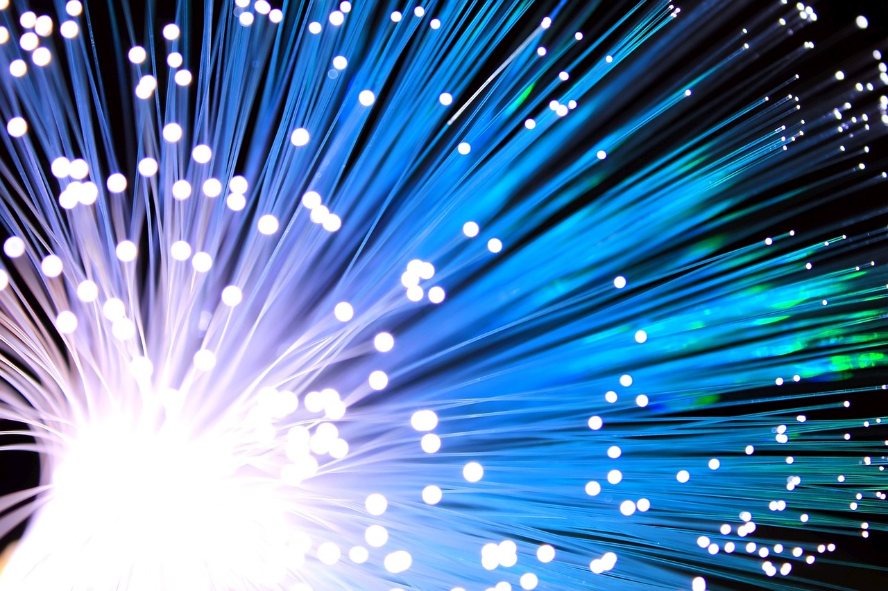
SiF4 in Specialty Glass: Enhancing Optical and Industrial Performance
SiF4’s precision extends to specialty glass, where it enhances optical clarity, durability, and performance in applications like fiber optics and UV-resistant windows. In optical fiber production, SiF4 dopes silica in vapor axial deposition (VAD), lowering the cladding’s refractive index to ensure total internal reflection. (Source: https://www.asiaisotopeintl.com/product/silicon-tetrafluoride-sif4/) This achieves ultra-low attenuation (0.15 dB/km), critical for 6G networks handling massive data. (Source: https://www.insightaceanalytic.com/report/next-generation-optical-fiber-market/2772)
High-purity SiF4 ensures impurity-free doping, preventing light scattering. Recent advances in multi-core fibers use SiF4 to fine-tune each core, boosting bandwidth by 10x. (Source: https://www.insightaceanalytic.com/report/next-generation-optical-fiber-market/2772) In specialty glass for semiconductor fabs, SiF4 creates UV-resistant windows that withstand harsh cleanroom conditions. (Source: https://www.metrowelding.com/silicon-tetrafluoride)
For optical coatings, SiF4 deposits thin fluoride layers via CVD, enhancing anti-reflective properties for lenses in lasers or telescopes. (Source: https://www.metrowelding.com/silicon-tetrafluoride) A 2025 patent highlights SiF4 in fluorinated glass for photonic circuits, integrating optics with electronics. (Source: https://patents.google.com/patent/US5872065) Vortex fibers, using SiF4 doping, support orbital angular momentum modes, multiplying data capacity. (Source: https://www.azooptics.com/Article.aspx?ArticleID=2765)
SiF4 also enhances industrial glass, like fluorosilicate glass for chemical resistance in reactors. (Source: https://www.wechemglobal.com/high-purity-silicon-tetrafluoride-gas-sif4-fluorocarbon-gases-product/) These applications drive the specialty glass market, valued at $2.8 billion in 2024, with a 7% CAGR through 2030. (Source: https://www.grandviewresearch.com/industry-analysis/specialty-glass-market)
Safety and Environmental Considerations
SiF4 is toxic and corrosive, producing HF upon hydrolysis, which can cause severe burns and respiratory issues. (Source: https://nj.gov/health/eoh/rtkweb/documents/fs/1667.pdf) Handle it with PPE, including self-contained breathing apparatus, in well-ventilated areas. (Source: https://amp.generalair.com/MsdsDocs/PA46522S.pdf)
Environmentally, its volatility limits persistence, but emissions can acidify soil and water. (Source: https://cameochemicals.noaa.gov/chemical/1449) EPA and EU regulations mandate scrubbers to neutralize HF, and 2025 PFAS rules push recycling. (Source: https://www.semiconductors.org/wp-content/uploads/2023/06/FINAL-Plasma-Etch-and-Deposition-White-Paper.pdf) Closed-loop systems cut emissions by 50%, aligning with net-zero goals. (Source: https://archivedproceedings.econference.io/wmsym/2000/pdf/31/31-07.pdf)
Market Trends and Future Innovations
The SiF4 market, valued at $2.5 billion in 2024, is set to reach $3.6 billion by 2032 at 4.3% CAGR, driven by semiconductors and optics. (Source: https://www.acumenresearchandconsulting.com/silicon-tetrafluoride-market) High-purity segments grow at 8.8% to $2.5 billion by 2033. (Source: https://www.verifiedmarketreports.com/product/silicon-tetrafluoride-market/)
Innovations include AI-driven etching optimization, reducing defects by 10%. (Source: https://pubs.aip.org/avs/jvb/article/42/4/041501/3297248/Future-of-plasma-etching-for-microelectronics) Cryogenic etching adoption for 3D NAND could dominate by 2026. (Source: https://kovismi.com/cryogenic-etching-the-key-to-3d-semiconductor-transformation/) In glass, SiF4-doped perovskites for solar cells promise 30% efficiency gains. (Source: https://www.pv-magazine.com/2025/01/07/fluorine-doping-for-perovskite-solar-cells/)
By 2030, SiF4 could enable 1nm chips and quantum-grade glass, with patents exploring wasterless synthesis. (Source: https://portal.unifiedpatents.com/patents/patent/US-10784102-B2)
Conclusion
SiF4’s precision in semiconductor etching, deposition, and specialty glass production is unlocking new frontiers in high-tech manufacturing. Its high-purity applications drive efficiency, sustainability, and innovation, powering AI chips and next-gen optics. As industries evolve, SiF4’s role will expand, shaping a precise, connected future.
Would you like a deeper dive into any specific technical parameters or applications ?
As an industry leader focused in specialty gases , our goal is to support our customers by keeping them at the forefront of their industries. We’re here to help with any questions you might have so you can transform your ideas into reality, and tackle those big science challenges.
Get free consultant, our experts are ready to serve.
(Follow up our update artiles on www.asiaisotopeintl.com or send your comments to tao.hu@asiaisotope.com for further communications )