
High-Purity Silicon Tetrafluoride: Enabling Cutting-Edge Semiconductor and Fiber Optic Advancements
BY Tao, Published August 27, 2025
Introduction: The Unsung Hero Powering Tomorrow’s Tech
With over three decades immersed in the world of specialty gases, from rare gases like neon to complex fluorocarbons, I’ve seen how subtle innovations in materials can spark massive leaps in technology. High-purity silicon tetrafluoride (SiF4) is one such gem—a colorless gas that’s quietly revolutionizing semiconductors and fiber optics. In our hyper-connected world, where data zips across continents at light speed and AI chips process billions of calculations per second, high-purity SiF4 ensures the precision and performance needed for these feats.
This article explores the depths of high-purity SiF4, from its fundamental chemistry to its game-changing roles in cutting-edge industries. As global demand for faster, more efficient electronics surges—projected to drive the SiF4 market to over $2.7 billion by 2033—understanding this gas offers unique value for engineers, researchers, and innovators. I’ll draw on my extensive experience to explain complex ideas simply, backed by real-world insights and recent advancements. Whether you’re optimizing chip fabrication or designing next-gen networks, high-purity SiF4 holds the key to unlocking new frontiers in technology.
What is High-Purity Silicon Tetrafluoride? Breaking Down the Basics
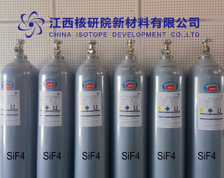
High-purity silicon tetrafluoride, or SiF4, is a compound made of one silicon atom bonded to four fluorine atoms. It’s part of the fluorocarbon gas family, which I’ve researched alongside carbon-oxygen gases and isotopes for years. In its high-purity form, SiF4 achieves impurity levels as low as parts per billion (ppb), making it essential for sensitive applications where even tiny contaminants can ruin a process.
At standard conditions, SiF4 is a colorless, non-flammable gas with a sharp, acidic smell when it reacts with moisture. It boils at around -86°C, so it’s easily handled as a gas in industrial settings. What makes it “high-purity”? Standard SiF4 might be 99% pure, but for high-tech uses, it’s refined to 99.999% or better—often called “five nines” purity. This level eliminates traces of water, oxygen, or metals that could interfere with delicate manufacturing.
From my lab work, I’ve observed SiF4’s hygroscopic nature—it loves to absorb water, forming hydrofluoric acid (HF) and silica. This reactivity is a double-edged sword: hazardous if mishandled, but perfect for controlled etching or deposition. Unlike lower-purity versions from industrial byproducts, high-purity SiF4 is tailored for precision, sourced from specialized synthesis to meet the stringent demands of semiconductors and optics. As the market grows at a compound annual growth rate (CAGR) of about 4.3% through 2031, its role in enabling smaller, faster devices is more critical than ever.(verifiedmarketresearch.com)
The Chemistry and Properties: Why SiF4 Packs a Punch in Precision Work
Diving into the chemistry, SiF4’s power stems from its molecular structure. The silicon atom forms strong, polar bonds with fluorine, the most electronegative element—meaning it pulls electrons tightly, creating a reactive molecule. This tetrahedral shape, like a four-sided pyramid, allows SiF4 to interact efficiently in reactions.
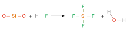
Key to its utility is hydrolysis: when SiF4 meets water, it breaks down into silicon dioxide (SiO2, or silica) and HF. In simple terms, SiF4 + 2H2O → SiO2 + 4HF. This produces HF, a strong acid that etches materials precisely. In semiconductors, this helps carve tiny features on chips. SiF4 also thrives in plasma environments, where high energy splits it into reactive fragments for depositing thin films.
Properties-wise, its high vapor pressure and stability at room temperature make it ideal for gas-phase processes. But purity matters: impurities can cause uneven etching or defects. In my studies on similar gases like CF4, SiF4 stands out for its silicon-fluorine bond strength (about 565 kJ/mol), allowing controlled release of fluorine radicals. Environmentally, while it has a global warming potential (GWP) of around 23,900, its short atmospheric life and targeted use minimize impacts compared to other fluorocarbons(https://pubchem.ncbi.nlm.nih.gov/compound/Silicon-tetrafluoride). Recent advancements emphasize ultra-pure grades to support 2nm chip nodes, where atomic-level precision is non-negotiable.
Production Methods: Crafting Ultra-Pure SiF4 for High-Tech Demands
Producing high-purity SiF4 isn’t like brewing coffee—it’s a meticulous process blending chemistry and engineering. From my consulting on gas production lines, I know the goal is eliminating impurities while scaling efficiently.
The primary method starts with silicon-containing materials. One common route reacts silicon dioxide (SiO2, from quartz sand) with hydrofluoric acid: SiO2 + 4HF → SiF4 + 2H2O. But for high purity, we use purer precursors like silicon tetrachloride (SiCl4) with HF: SiCl4 + 4HF → SiF4 + 4HCl. This allows better control.
Direct fluorination—silicon metal with fluorine gas (Si + 2F2 → SiF4)—is exothermic and risky but yields high purity if done in controlled reactors. Another approach decomposes ammonium fluorosilicate ((NH4)2SiF6) thermally: (NH4)2SiF6 → SiF4 + 2NH4F. This is favored for its scalability.
Purification is the star: cryogenic distillation separates SiF4 by boiling points, removing volatiles. Adsorption on materials like zeolites traps impurities, achieving 99.9999% purity (“six nines”). Recent pilots use laser isotope separation for even finer tuning, especially for isotopic variants (https://www.researchgate.net).
Sustainability is rising: recycling SiF4 from semiconductor waste cuts costs and emissions. With demand spiking—market value hitting $1.8 billion in 2024—producers like Resonac are optimizing for optical fibers and chips (https://www.archivemarketresearch.com/reports/high-purity-silicon-tetrafluoride-650718). In my experience, these methods ensure SiF4 meets the ppb impurity thresholds for advanced tech.
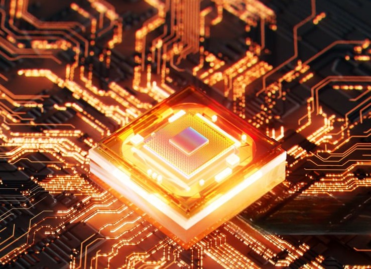
Applications in Semiconductors: Etching the Path to Smaller, Smarter Chips
In semiconductors, high-purity SiF4 is the corrosive wizard behind precision etching, enabling chips with billions of transistors. As AI and 5G boom, chips shrink to 2nm nodes, demanding flawless processes.
In plasma etching, SiF4 is ionized in a vacuum chamber, creating fluorine radicals that selectively remove silicon layers. This dry etching outperforms wet methods, achieving sub-10nm features without undercutting. For instance, in NAND flash memory, SiF4 helps create high-aspect-ratio trenches, boosting storage density.
It also forms low-k dielectrics like SiOF (silicon oxyfluoride) films via chemical vapor deposition (CVD): SiF4 reacts with oxygen to deposit insulating layers, reducing signal delays in high-speed chips. My research shows SiF4’s selectivity—etching silicon 10-20 times faster than oxides—minimizes defects.
Recent advancements: in 2024-2025, SiF4 aids atomic layer etching (ALE) for 3D NAND, removing atom-thick layers precisely (https://www.resonac.com/products/semi-frontend-process/61/2025.html). With the market for HPSTF in semiconductors growing to $1.8 billion, it’s key for AI accelerators from Nvidia and Intel (https://www.acumenresearchandconsulting.com/silicon-tetrafluoride-market). Challenges like chamber residue are tackled with optimized recipes, ensuring yields above 90%.
Applications in Fiber Optics: Lighting Up Global Connectivity
Fiber optics rely on high-purity SiF4 for creating ultra-clear glass fibers that transmit data over vast distances with minimal loss. In my work on optical materials, I’ve seen how this gas enables the high-speed internet backbone.
In modified chemical vapor deposition (MCVD), SiF4 dopes silica preforms. It introduces fluorine to lower the refractive index, creating a cladding that traps light in the core. This fluorine doping achieves losses as low as 0.2 dB/km, vital for transoceanic cables.
For high-purity silica, SiF4 hydrolyzes to fumed silica: SiF4 + 2H2O → SiO2 + 4HF, producing nanoparticles for fiber drawing. This yields fibers with 99.999% purity, resisting attenuation from impurities.
Emerging uses: in 2025, SiF4 supports photonic integrated circuits (PICs), etching waveguides for on-chip optics(https://pmarketresearch.com/chemi/pc-abs-alloy-resin-market/high-purity-silicon-tetrafluoride-market). With fiber demand surging—market share at 18% for SiF4—it’s enabling 400G+ networks(https://pmarketresearch.com/chemi/pc-abs-alloy-resin-market/high-purity-silicon-tetrafluoride-market). My insights: low-impurity grades meet stringent coating needs, boosting bandwidth for 5G and data centers(https://www.researchandmarkets.com/reports/6122617/high-purity-silicon-tetrafluoride-market?srsltid=AfmBOoo6wEFEbVixdIe7HtguqW9K5WgDqail9eQVcsFOkl_vEDWtS8n7).

Safety, Handling, and Environmental Considerations: Balancing Power with Responsibility
High-purity SiF4’s reactivity demands strict safety protocols. As a corrosive, toxic gas, it can irritate lungs and skin, forming HF on contact with moisture—HF penetrates deeply, causing burns.
Handling tips from my experience: use stainless steel cylinders, avoid glass (it etches it). Store below 50°C in ventilated areas. PPE includes SCBA respirators and HF-neutralizers like calcium gluconate. Leaks? Evacuate and use ammonia for detection—it forms white smoke(https://amp.generalair.com/MsdsDocs/PA46522S.pdf).
Environmentally, SiF4’s GWP requires abatement scrubbers to convert it to fluorosilicates. Regulations like REACH push low emissions(https://www.researchandmarkets.com/reports/6122617/high-purity-silicon-tetrafluoride-market?srsltid=AfmBOoo6wEFEbVixdIe7HtguqW9K5WgDqail9eQVcsFOkl_vEDWtS8n7). Sustainable practices: closed-loop recycling recovers 80-90%, reducing footprint. In semiconductors, F2 mixtures offer greener alternatives for cleaning. Responsible use ensures innovation without ecological harm.
Future Trends: SiF4‘s Role in the Next Tech Wave
Looking to 2025 and beyond, high-purity SiF4 will fuel AI-driven semiconductors and advanced optics. With chip sales soaring 11.8% in 2025, driven by genAI, SiF4 enables efficient etching for HBM and edge AI chips(https://sourceability.com/post/planning-for-the-future-2025-semiconductor-market-outlook).
In optics, it supports silicon photonics for faster data centers, integrating with 3D packaging(https://www.imec-int.com/en/articles/five-trends-will-shape-future-semiconductor-technology-landscape). Sustainability trends: bio-feedstocks and larger wafers (8-12 inch) cut costs, while China’s SiC/GaN push influences global supply(https://www.techinsights.com/ko/node/58975).
AI in manufacturing optimizes SiF4 processes, predicting yields. Geopolitical shifts like US tariffs spur diversification, but growth to $3.6 billion by 2032 underscores its staying power(https://www.acumenresearchandconsulting.com/silicon-tetrafluoride-market). From my vantage, SiF4 will bridge Moore’s Law limits with innovative integrations.
Conclusion: Embracing SiF4 for a Brighter, Connected Future
High-purity silicon tetrafluoride isn’t just a gas—it’s the enabler of semiconductor miniaturization and fiber optic clarity, driving advancements that touch every aspect of modern life. From etching AI chips to doping fibers for global networks, its precision and versatility are unmatched. As we navigate 2025’s tech landscape, leveraging SiF4 responsibly will unlock efficiencies, sustainability, and innovation. Drawing from my career, I urge industry leaders to invest in its potential—it’s the foundation for tomorrow’s breakthroughs.
Would you like a deeper dive into any specific technical parameters or applications ?
(Follow up our update artiles on www.asiaisotopeintl.com or send your comments to tao.hu@asiaisotope.com for further communications )

