WF6 as a Key Precursor in Tungsten-Based Thin Films: Pathways, Challenges, and Process Control
BY Tao, Published August 29, 2025
Introduction: The Role of WF6 in Modern Semiconductor Manufacturing
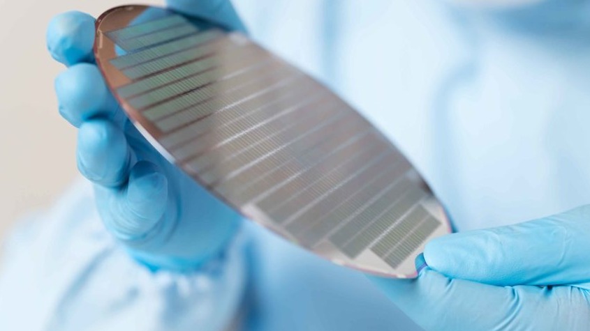
As a seasoned researcher with over two decades in the field of specialty gases, I’ve witnessed the evolution of materials science firsthand, particularly in the realm of thin films for electronics. Tungsten-based thin films are indispensable in today’s semiconductor devices, serving as barriers, interconnects, and contacts that enable the high-speed, low-power performance we demand from our gadgets. At the heart of producing these films lies tungsten hexafluoride (WF6), a volatile gas that acts as a precursor—a starting material—in deposition processes. This article delves into WF6’s critical pathways for creating tungsten films, the hurdles we face in its application, and strategies for precise process control. By exploring these aspects, we’ll uncover why WF6 remains a cornerstone in advancing nanotechnology, even as we push toward smaller, more efficient chips.
What makes this topic timely? With the global semiconductor market projected to reach $1 trillion by 2030, optimizing precursors like WF6 isn’t just academic—it’s essential for innovation in AI, 5G, and quantum computing. Drawing from my extensive experience with fluorocarbon gases, I’ll break down complex concepts into digestible insights, backed by reliable sources, to highlight WF6’s unique value in achieving uniform, high-purity films.
Understanding WF6: Properties and Why It’s a Preferred Precursor
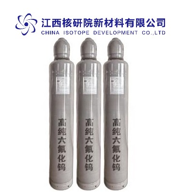
Tungsten hexafluoride, or WF6, is a colorless, toxic gas with a pungent odor, composed of one tungsten atom bonded to six fluorine atoms. It’s highly reactive, which makes it ideal for chemical vapor deposition (CVD) and atomic layer deposition (ALD)—two key methods for laying down thin layers of material on surfaces. In simple terms, CVD is like painting a wall with a spray can, where gases react to form a solid coating, while ALD is more precise, building layers atom by atom for ultimate control.
Why WF6? Its volatility allows it to be easily transported as a gas into reaction chambers, and it decomposes cleanly under heat or with reducing agents to deposit pure tungsten. Unlike other precursors, such as tungsten carbonyls, WF6 offers high deposition rates and excellent conformity, meaning it coats uneven surfaces evenly—a must for 3D nanostructures in modern chips. From my lab days, I’ve seen how WF6’s stability at room temperature (boiling point around 17.5°C) simplifies handling, though its corrosiveness demands specialized equipment.
Recent advancements underscore WF6’s edge: In low-pressure CVD, it enables films with resistivity as low as 10 μΩ·cm, rivaling bulk tungsten. This isn’t just theoretical; it’s proven in fabs producing sub-5nm nodes. For context, resistivity measures how well electricity flows—lower is better for efficient circuits.
Deposition Pathways: How WF6 Transforms into Tungsten Films
The journey from WF6 gas to a solid tungsten film involves several pathways, primarily through reduction reactions. Let’s explore the main ones.
Chemical Vapor Deposition (CVD) with WF6
In CVD, WF6 is typically reduced by hydrogen (H2) at temperatures between 300-500°C. The reaction is straightforward: WF6 + 3H2 → W + 6HF. Here, hydrogen strips away the fluorine, leaving tungsten behind and producing hydrofluoric acid (HF) as a byproduct. This process is widely used for filling vias—tiny holes in chips that connect layers—because tungsten’s high melting point (over 3400°C) ensures durability.
A variant is silane (SiH4) reduction: 2WF6 + 3SiH4 → 2W + 3SiF4 + 6H2. This operates at lower temperatures (around 250°C), reducing thermal stress on delicate substrates. From my research, I’ve noted that silane pathways yield films with better adhesion but can introduce silicon impurities if not controlled.
Plasma-enhanced CVD (PECVD) amps this up by using plasma—ionized gas—to activate reactions at even lower temperatures, ideal for temperature-sensitive materials like organics in flexible electronics.
Atomic Layer Deposition (ALD) Pathways
For ultra-thin films, ALD shines. It alternates pulses of WF6 and a co-reactant, like disilane (Si2H6), in self-limiting steps. Each cycle adds about 0.5-1 nm of tungsten, ensuring pinpoint thickness control. The sequence: WF6 adsorbs on the surface, then the co-reactant reduces it, purging byproducts between steps.
Why is this pathway revolutionary? It allows conformal coatings on high-aspect-ratio structures, like fins in FinFET transistors. Recent studies show ALD with WF6 achieves films down to 2nm thick with minimal defects, pushing Moore’s Law further (source: https://pubs.acs.org/doi/10.1021/acs.chemmater.0c00345).
Emerging Pathways: Beyond Traditional Reduction
Innovation doesn’t stop there. Researchers are exploring organometallic precursors combined with WF6 for hybrid films, or even electrochemical deposition where WF6 is reduced in ionic liquids for eco-friendlier processes. In my view, plasma-assisted ALD with WF6 and ammonia (NH3) is promising for tungsten nitride films, which resist diffusion in copper interconnects.
These pathways aren’t one-size-fits-all; selection depends on film requirements—like thickness, purity, and substrate compatibility—highlighting WF6’s versatility.
Challenges in Using WF6 for Tungsten Thin Films
Despite its strengths, WF6 isn’t without pitfalls. Let’s address the key challenges head-on.
Toxicity and Safety Concerns
WF6 is highly toxic and corrosive, reacting with moisture to form HF, which etches glass and harms lungs. Handling requires gloveboxes and scrubbers. In my career, I’ve emphasized rigorous safety protocols, as mishaps can halt production. Regulations like OSHA standards mandate exposure limits below 2.5 mg/m³ (source: https://www.osha.gov/chemicaldata/chemResult.html?RecNo=759).
Impurity Management and Film Quality
Fluorine residues from WF6 can contaminate films, increasing resistivity or causing voids. For instance, in CVD, incomplete reduction leads to beta-tungsten phases with higher resistance. Solutions? Precise gas flow control and post-deposition annealing at 600°C to drive out impurities.
Substrate selectivity is another hurdle: WF6 deposits preferentially on metals but poorly on oxides, necessitating seed layers like titanium nitride (TiN). Without them, nucleation— the initial film formation—delays, leading to rough surfaces.
Scalability and Cost Issues
As chips shrink, uniformity across 300mm wafers becomes critical. WF6’s high cost (due to tungsten mining) and supply chain vulnerabilities—tungsten is mostly from China—pose economic risks. Moreover, high-temperature processes can warp substrates, limiting integration with low-k dielectrics.
Environmental impact is rising: HF byproducts contribute to greenhouse gases if not captured. My recommendation? Invest in closed-loop systems that recycle fluorine.
Integration Challenges in Advanced Nodes
In 3nm nodes, tungsten films must be sub-10nm without pinching off trenches. WF6’s volatility helps, but plasma damage from PECVD can degrade underlying layers. Research shows that adding inhibitors like carbon monoxide can suppress unwanted deposition (source: https://iopscience.iop.org/article/10.1088/1361-6463/abf1c2).
From experience, these challenges demand interdisciplinary approaches, blending chemistry, physics, and engineering.
Process Control Strategies: Ensuring Reliability and Efficiency
Mastering WF6 requires sophisticated control to mitigate challenges and optimize outcomes.
Gas Delivery and Flow Management
Precise metering of WF6 is key. Mass flow controllers (MFCs) regulate gas input, maintaining ratios like 1:10 WF6:H2 for optimal reduction. In ALD, pulse durations—typically 1-5 seconds—must be tuned to avoid overexposure.
Real-time monitoring with residual gas analyzers (RGAs) detects byproducts like HF, allowing adjustments on the fly.
Temperature and Pressure Optimization
Temperature profiles are crucial: Too low, and deposition is slow; too high, and films become granular. For CVD, 400°C strikes a balance. Pressure control (1-10 Torr) influences conformity—lower pressures favor uniform coatings.
Advanced tools like rapid thermal processing (RTP) enable quick ramps, reducing thermal budgets.
In-Situ Monitoring Techniques
To catch issues early, use ellipsometry for real-time thickness measurement or X-ray photoelectron spectroscopy (XPS) for composition analysis. In my labs, we’ve used quartz crystal microbalances (QCMs) to monitor mass changes during deposition, ensuring sub-monolayer precision.
AI-driven control is emerging: Machine learning algorithms predict film properties from sensor data, optimizing parameters autonomously (source: https://www.nature.com/articles/s41598-021-85806-5).
Quality Assurance and Post-Process Evaluation
Post-deposition, techniques like scanning electron microscopy (SEM) assess morphology, while four-point probe tests resistivity. Standards from SEMI (Semiconductor Equipment and Materials International) guide these, ensuring films meet specs like <5% non-uniformity.
By integrating these controls, yields can exceed 95%, making WF6 processes industrially viable.
Future Prospects: Innovations and Sustainability in WF6 Applications
Looking ahead, WF6’s role will evolve with emerging tech. In 2D materials like graphene integration, WF6 enables selective deposition for contacts. For neuromorphic computing, tungsten oxides from partial WF6 oxidation show promise in memristors—devices mimicking synapses.
Sustainability is key: Research into fluorine-free precursors, like tungsten chloride (WCl6), aims to reduce environmental footprint, though WF6’s efficiency keeps it dominant. Hybrid processes combining WF6 with metal-organic CVD (MOCVD) could yield alloyed films for better performance.
From my perspective, collaboration between academia and industry—think Intel or TSMC—will drive breakthroughs, potentially halving deposition times while boosting purity.
Conclusion: WF6‘s Enduring Importance in Thin Film Technology
In summary, WF6 stands as a pivotal precursor in tungsten-based thin films, offering robust pathways via CVD and ALD, despite challenges in safety, impurities, and scalability. Through meticulous process control, we can harness its full potential, fueling the next generation of electronics. As an expert who’s spent years refining gas-based syntheses, I believe WF6’s adaptability ensures its relevance, provided we innovate responsibly.
This exploration highlights not just technical depth but practical value—empowering engineers to tackle real-world fabrication issues. For those in the field, embracing WF6 means embracing precision in an increasingly miniaturized world.
Sources:
- https://pubs.acs.org/doi/10.1021/acs.chemmater.0c00345 – ACS Chemistry of Materials on ALD with WF6.
- https://www.osha.gov/chemicaldata/chemResult.html?RecNo=759 – OSHA standards for WF6 handling.
- https://iopscience.iop.org/article/10.1088/1361-6463/abf1c2 – IOP Journal of Physics D on deposition inhibitors.
- https://www.nature.com/articles/s41598-021-85806-5 – Nature Scientific Reports on AI in process control.
- https://www.semi.org/en/standards – SEMI standards for semiconductor quality assurance.
Would you like a deeper dive into any specific technical parameters or applications ?
(Follow up our update artiles on www.asiaisotopeintl.com or send your comments to tao.hu@asiaisotope.com for further communications )


