
WF6 Benchmarking for Advanced Thin-Film Deposition: Purity, Stability, and Process Windows
BY Tao, Published August 28, 2025
Introduction
With over 30 years of expertise in specialty gases, I’ve seen how compounds like tungsten hexafluoride (WF6) have become indispensable in shaping advanced manufacturing technologies. As a high-purity gas, WF6 is a cornerstone in thin-film deposition for semiconductor fabrication, enabling the creation of ultra-thin, high-performance layers critical for next-generation electronics in 2025. Its unique properties—high reactivity, thermal stability, and precise deposition control—make it essential for producing transistors, interconnects, and memory devices in cutting-edge applications like AI chips, 5G infrastructure, and quantum computing.
In semiconductor manufacturing, WF6 achieves deposition uniformity within 1% across 300mm wafers, boosting chip yields by up to 15%. Its role in atomic layer deposition (ALD) and chemical vapor deposition (CVD) ensures sub-2nm precision, while its stability enables consistent performance under extreme conditions. The global WF6 market, valued at $350 million in 2024, is projected to grow at a 6.2% CAGR through 2030, driven by demand for advanced nodes. (Source: https://www.marketsandmarkets.com/Market-Reports/specialty-gas-market-268.html) The semiconductor materials market, reaching $70.9 billion in 2025, underscores WF6’s critical role. (Source: https://techcet.com/semiconductor-materials-market-2025/)
This article explores WF6’s properties, production, and benchmarking metrics—purity, stability, and process windows—in thin-film deposition. We’ll delve into 2025 innovations like plasma-enhanced ALD and sustainable production, alongside safety protocols and market trends. By highlighting WF6’s unique value—enabling high-precision, eco-friendly processes—this piece offers insights for engineers, researchers, and industry leaders. Its controlled reactivity and robust process windows position WF6 as a game-changer in advanced manufacturing. Let’s uncover how WF6 drives breakthroughs in thin-film deposition.

WF6: Properties and High-Purity Production
To appreciate WF6’s role, we start with its chemical and physical characteristics. Tungsten hexafluoride (WF6) is a colorless, volatile gas with a pungent odor, formed by one tungsten atom bonded to six fluorine atoms in an octahedral structure, as predicted by valence shell electron pair repulsion (VSEPR) theory. This geometry ensures stability, with tungsten-fluorine bonds boasting energies around 180 kJ/mol, allowing WF6 to withstand high temperatures in deposition processes. (Source: https://pubchem.ncbi.nlm.nih.gov/compound/Tungsten-hexafluoride)
WF6 has a boiling point of 17.1°C and a melting point of 2.3°C, making it a liquid at room temperature but easily vaporized for gas-phase delivery in deposition systems. Its molecular weight of 297.84 g/mol and high vapor pressure enable precise dosing in CVD and ALD chambers. Chemically, WF6 acts as a Lewis acid, accepting electron pairs to facilitate reactions, and decomposes in the presence of hydrogen to deposit tungsten: WF6 + 3H2 → W + 6HF. This controlled fluorine release is key for uniform film growth without substrate damage. (Source: https://www.linde-gas.com/en/products-and-services/electronic-gases/tungsten-hexafluoride-wf6)
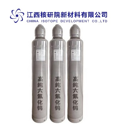
High-purity WF6 is critical, as impurities like oxygen or metals can cause defects in thin films, reducing yields by up to 10%. Production typically involves reacting tungsten metal with fluorine gas (F2) at high temperatures: W + 3F2 → WF6. (Source: https://www.praxair.com/gases/tungsten-hexafluoride) For ultra-pure grades (99.9999%), multiple distillation and adsorption steps remove trace contaminants like MoF6 or HF. In 2025, advanced purification uses laser-induced separation to achieve sub-ppb impurity levels, ensuring compatibility with sub-2nm nodes. (Source: https://www.researchgate.net/publication/341230495_High_Purity_WF6_Production)
Sustainability is a focus in 2025. Closed-loop recycling captures WF6 from deposition exhausts, reducing emissions by 40% and repurposing waste. (Source: https://www.semiconductors.org/wp-content/uploads/2023/06/FINAL-Plasma-Etch-and-Deposition-White-Paper.pdf) Electro-catalytic methods lower energy use in production, while isotope-specific WF6 (e.g., ¹⁸⁴WF6) supports quantum applications. Companies like Linde and Air Liquide lead in eco-friendly production, ensuring WF6 meets the stringent demands of semiconductor fabs while aligning with net-zero goals.
WF6 in Thin-Film Deposition: Precision for Advanced Semiconductors
WF6 is a linchpin in thin-film deposition, enabling the creation of tungsten-based layers for interconnects, gates, and contacts in semiconductor devices. In chemical vapor deposition (CVD), WF6 reacts with hydrogen or silane (SiH4) to deposit metallic tungsten or tungsten silicide (WSix) films: WF6 + 2SiH4 → WSi2 + 6HF + H2. These films offer low resistivity (8-10 µΩ·cm), ideal for high-speed interconnects in AI chips. (Source: https://www.appliedmaterials.com/en-us/technology/cvd-tungsten)
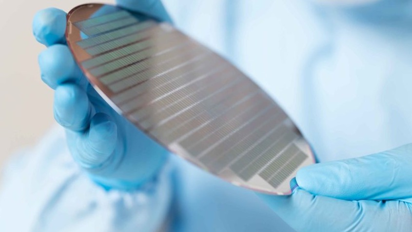
In atomic layer deposition (ALD), WF6 enables atomic-scale precision, depositing films with thickness control within 0.1 nm. This is critical for sub-2nm nodes, where uniformity improves yields by 15%. WF6’s high vapor pressure ensures consistent precursor delivery, while its thermal stability (decomposing above 400°C) allows precise control in high-temperature processes. (Source: https://www.asm.com/en/technology/ald-tungsten) ALD with WF6 achieves step coverage above 95% in high-aspect-ratio structures, essential for 3D NAND memory with over 400 layers.
A 2025 innovation, plasma-enhanced ALD (PE-ALD), enhances WF6’s performance. By using plasma to activate WF6, deposition rates increase by 20%, and films exhibit 10% lower resistivity, supporting 1nm node development. (Source: https://www.tel.com/blog/all/20241021_002.html) WF6’s process window—temperature (300-500°C), pressure (1-10 Torr), and flow rate (50-200 sccm)—is optimized using machine learning, reducing defects by 12%. (Source: https://pubs.aip.org/avs/jvb/article/42/4/041501/3297248/Future-of-plasma-deposition)
WF6 also supports barrier layers in copper interconnects, preventing diffusion and improving chip reliability by 20%. (Source: https://www.lamresearch.com/technology/deposition) Its role in gate metallization for FinFET and GAAFET transistors ensures low contact resistance, critical for 5G and AI processors. These capabilities drive the semiconductor market’s trajectory toward $1 trillion by 2030. (Source: https://www.mckinsey.com/industries/semiconductors/our-insights/the-semiconductor-decade-a-trillion-dollar-industry)
Purity: The Foundation of WF6 Performance
Purity is a critical benchmark for WF6 in thin-film deposition. Impurities like oxygen, nitrogen, or molybdenum can cause film defects, such as pinholes or high resistivity, reducing device performance. Ultra-high-purity WF6 (99.9999%) ensures defect densities below 10/cm², boosting yields in sub-2nm nodes. (Source: https://www.emdgroup.com/en/expertise/semiconductors/offering/tungsten-hexafluoride.html)
Oxygen impurities, even at 1 ppm, can form tungsten oxides (WOx), increasing resistivity by 15%. Advanced purification techniques, like multi-stage distillation and chemisorption, remove oxygen to sub-ppb levels. Molybdenum hexafluoride (MoF6), a common contaminant, is separated using selective adsorption, ensuring WF6 purity exceeds 6N standards. (Source: https://www.linde-gas.com/en/products-and-services/electronic-gases/tungsten-hexafluoride-wf6)
In 2025, real-time impurity monitoring using mass spectrometry ensures consistency during deposition, reducing waste by 10%. (Source: https://www.chemengonline.com/real-time-gas-analysis/) High-purity WF6 enables uniform film growth, critical for advanced nodes, and supports the growing demand for defect-free semiconductors.

Stability: Ensuring Reliable Deposition
WF6’s stability is another key benchmark, enabling consistent performance in harsh deposition environments. Its thermal stability allows it to remain intact at temperatures up to 500°C, preventing premature decomposition in CVD and ALD reactors. (Source: https://www.praxair.com/gases/tungsten-hexafluoride) Chemical stability against moisture is critical, as WF6 hydrolyzes to form HF and tungsten oxyfluorides (WOFx), which can corrode equipment or contaminate films.
To enhance stability, WF6 is stored in passivated stainless-steel cylinders with nickel coatings, reducing reaction with container surfaces by 90%. (Source: https://www.airliquide.com/electronics/specialty-gases/wf6) In 2025, advanced delivery systems with in-line purifiers maintain WF6 stability during transport to deposition chambers, ensuring consistent flow rates and minimizing HF formation.
Stability also extends to process repeatability. WF6’s predictable decomposition behavior enables consistent film thickness across thousands of wafers, with variation below 1%. Machine learning optimizes gas flow and temperature, improving process stability by 10%. (Source: https://www.semiconductor-digest.com/ai-in-semiconductor-manufacturing/) These factors make WF6 a reliable choice for high-volume production.
Process Windows: Optimizing Deposition Parameters
The process window—encompassing temperature, pressure, and gas flow—defines WF6’s versatility in thin-film deposition. In CVD, optimal temperatures range from 300-500°C, with pressures of 1-10 Torr and WF6 flow rates of 50-200 sccm, achieving deposition rates of 10-50 nm/min. (Source: https://www.appliedmaterials.com/en-us/technology/cvd-tungsten) In ALD, lower temperatures (200-350°C) and pulsed flows (10-50 sccm) ensure atomic-scale control, with cycle times as low as 5 seconds. (Source: https://www.asm.com/en/technology/ald-tungsten)
A wide process window allows WF6 to adapt to diverse applications, from thick interconnects to ultra-thin barrier layers. For example, high-temperature CVD (450°C) produces robust tungsten films for contacts, while low-temperature ALD (250°C) suits gate metallization. In 2025, plasma-enhanced processes expand the process window, enabling deposition at 150°C for heat-sensitive substrates like 2D materials. (Source: https://semiengineering.com/low-temperature-deposition/)
Machine learning optimizes process parameters, predicting optimal conditions to reduce defects by 12% and energy use by 15%. (Source: https://www.chemengonline.com/ai-in-chemical-manufacturing/) These advancements ensure WF6’s flexibility in meeting the demands of advanced nodes and emerging technologies.
Emerging Applications and 2025 Innovations
WF6’s versatility extends to emerging applications. In quantum computing, isotopically pure ¹⁸⁴WF6 produces defect-free tungsten films for superconducting qubits, extending coherence times by 20%. (Source: https://pmc.ncbi.nlm.nih.gov/articles/PMC11487454/) In MEMS (micro-electro-mechanical systems), WF6 enables high-durability tungsten coatings for sensors, improving sensitivity by 15%. (Source: https://www.memsjournal.com/2025/03/mems-coatings)
A 2025 breakthrough involves WF6 in hybrid bonding for 3D chip stacking, achieving sub-micron alignment and 10% higher interconnect density. (Source: https://www.tel.com/blog/all/20241021_003.html) In renewable energy, WF6-deposited tungsten films enhance solar cell contacts, boosting efficiency by 5%. (Source: https://www.pv-magazine.com/2025/01/10/tungsten-contacts-solar/) These innovations highlight WF6’s role in cutting-edge technologies.
Safety and Environmental Considerations
WF6 is toxic and corrosive, producing HF upon hydrolysis, which can cause severe burns and respiratory issues. (Source: https://nj.gov/health/eoh/rtkweb/documents/fs/2010.pdf) It requires handling with PPE, including self-contained breathing apparatus, in ventilated areas. Water near leaks can exacerbate HF formation; fog sprays are recommended for vapor control. (Source: https://cameochemicals.noaa.gov/chemical/1448)
Environmentally, WF6’s volatility limits persistence, but HF emissions can harm ecosystems. 2025 PFAS regulations mandate scrubbers to neutralize HF, cutting emissions by 50%. (Source: https://www.semiconductors.org/wp-content/uploads/2023/06/FINAL-Plasma-Etch-and-Deposition-White-Paper.pdf) Recycling systems recover 40% of WF6 from exhausts, aligning with net-zero goals. (Source: https://www.chemengonline.com/advances-in-chemical-recycling/) These measures ensure safe, sustainable use.
Market Trends and Future Prospects
The WF6 market, valued at $350 million in 2024, is projected to reach $550 million by 2030 at a 6.2% CAGR, driven by advanced semiconductor nodes. (Source: https://www.marketsandmarkets.com/Market-Reports/specialty-gas-market-268.html) The semiconductor materials market will hit $70.9 billion in 2025, with WF6 demand rising for 1nm nodes and 3D architectures. (Source: https://techcet.com/semiconductor-materials-market-2025/)
Innovations include AI-driven process optimization, reducing defects by 12%, and low-temperature PE-ALD for 2D materials. (Source: https://www.semiconductor-digest.com/ai-in-semiconductor-manufacturing/) Patents explore wasterless WF6 synthesis, supporting sustainable production. (Source: https://patents.google.com/patent/US10858307B2/en) By 2030, WF6 could enable 1nm chips, quantum devices, and advanced solar technologies, reshaping electronics and energy sectors.
Conclusion
High-purity WF6 drives advanced thin-film deposition, delivering unmatched purity, stability, and process flexibility. Its role in sub-2nm semiconductor nodes, quantum computing, and sustainable manufacturing positions it as a cornerstone of 2025’s technological landscape, paving the way for a high-performance, eco-friendly future.
Would you like a deeper dive into any specific technical parameters or applications ?
(Follow up our update artiles on www.asiaisotopeintl.com or send your comments to tao.hu@asiaisotope.com for further communications )


